Methods of manufacturing ceramic board and electronic device

a technology of electronic devices and ceramic boards, which is applied in the direction of manufacturing tools, dielectric characteristics, ceramic layered products, etc., can solve the problems of difficult production efficiency and facilities of individual devices, small dimension of ceramic electronic devices having circuit functions (conductor patterns), and inability to obtain flat ceramic boards. , to achieve the effect of preventing warpage, excellent electric and mechanical properties, and efficient manufacturing

Inactive Publication Date: 2010-05-13
TDK CORPARATION
View PDF3 Cites 4 Cited by
  • Summary
  • Abstract
  • Description
  • Claims
  • Application Information

AI Technical Summary

Benefits of technology

[0029]The ceramic board manufactured by the above method is flat, and has no firing stain, so that an electronic device, excellent in electric and mechanical properties, can efficiently be manufactured by dividing this ceramic board.
[0030]According to the present invention, it is possible to obtain a ceramic board wherein warpage is prevented and no firing stain appears. In addition, because of the above constitution, it is possible to obtain the above ceramic board easily and efficiently regardless of a material of the ceramic board, etc. By using such a ceramic board, an electronic device having good properties can efficiently be manufactured.

Problems solved by technology

However, a ceramic electronic device having circuit function (conductor pattern) is small in dimension, and difficult to manufacture in a form of an individual device in terms of production efficiency and facilities, etc.
However, when shrinkage at firing is uneven, a flat ceramic board cannot be obtained, and for instance, there may be found deformation (warpage) such that edges of the board is heaved in a direction opposite to the setter plate side.
When dividing the ceramic board with warpage to obtain individual cuboid chip parts, the parts located in the edges of the board become rhombic, which can no longer be products and also cause the other problem such as inaccurate solder-mounting in a component mounting step.
In this case, organic components (carbon residue) such as binder remained in the green ceramic board may not be removed smoothly, and cause a sudden and rapid exothermal reaction.
With such firing stain, in the ceramic electronic device in which a circuit is formed, conductive material constituting the circuit can swell and break, resulting in reduction in electric and mechanical properties.
However, in the method disclosed in the Japanese Unexamined Patent Publication H6-329976, the ordinary setter plate is arranged on the lower surface of the board, so that it can be predicted to cause firing stain due to exothermal reaction of carbon residue at firing.
Also, when using a board having high sintering temperature, it is necessary to produce a green sheet with material having higher sintering temperature than that of the board, so that it is sometimes difficult to select the material.
Also, since unsintered green sheet is used, it is inferior in handling in view of strength when carrying the board sandwiched between green sheets and loading the same into a furnace.
Also, in the method disclosed in the Japanese Unexamined Patent Publication 2003-2750, it is necessary to select the binder for the green sheet depending on the type of the binder included in the board, so that it is sometimes difficult to select the type of the binder.
Further, as in the Japanese Unexamined Patent Publication H6-329476, the use of unsintered green sheet may cause to be difficult to handle.

Method used


Image

  • Methods of manufacturing ceramic board and electronic device
  • Methods of manufacturing ceramic board and electronic device
  • Methods of manufacturing ceramic board and electronic device

Examples


example 1

Green Ceramic Board

[0075]First, ceramic material powder, glass material powder and organic vehicle were mixed and kneaded to prepare a green sheet paste. The organic vehicle included binder, organic solvent, and if needed, plasticizer, dispersant, etc.

[0076]Next, conductive powder, glass material powder and organic vehicle were mixed and kneaded to prepare a conductive paste. The organic vehicle included binder, organic solvent, and if needed, plasticizer, dispersant, etc.

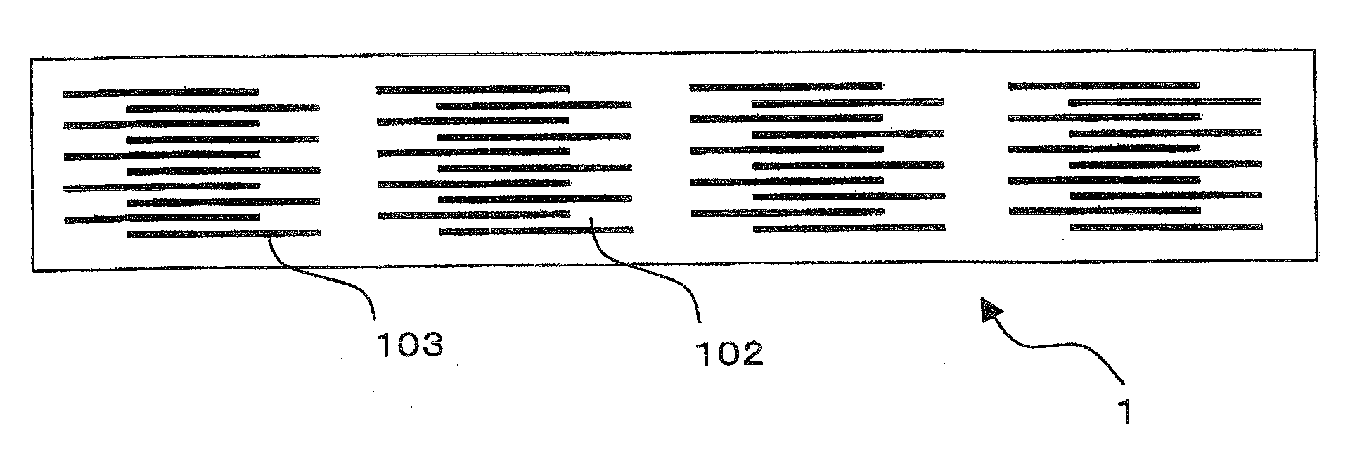
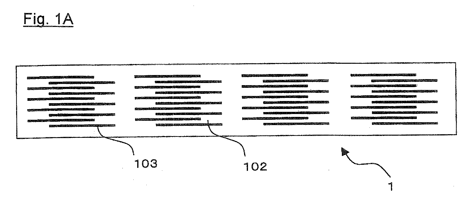
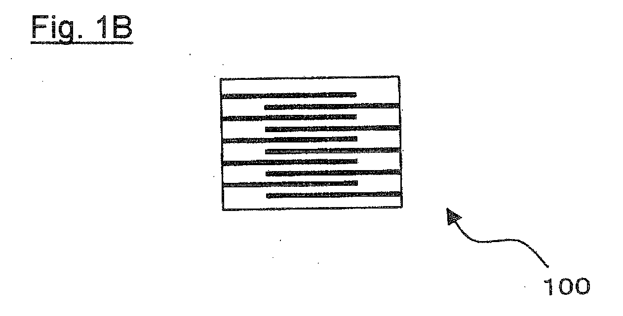
[0077]The above-obtained green sheet paste was coated on polymer film such as PET film by doctor blade method and dried. On the dried green sheet, the above-obtained conductive paste was printed and dried to produce a green sheet in which a conductor pattern having a thickness of 2.0±0.2 μm was formed.

[0078]A plurality of the above green sheets were produced and laminated to produce a green ceramic board which green chips to be electronic device elements were formed within.

[0079]Unit

[0080]As a fired porous ceramic ...

example 2

[0092]Except for changing the height of the void space provided between the bottom surface of the furnace and the honeycomb setter plate at the side of the lower surface of the green ceramic board to the value shown in Table 2, and changing the porosity of the honeycomb setter plate to 70%, a unit was formed, followed by each step of binder removal and firing, as in Example 1. For the warpage amount, the firing stain and the thickness of the internal electrode of the obtained ceramic board, same evaluations were done as in Example 1. The results are shown in Table 2.

TABLE 2Ceramic boardFiring stainVoid spaceWarpageThicknessSample No.[mm]amount [μm]of IE* [mm]100131No2.1110.595No1.812185No1.813280No1.714574No1.7151068No1.8165065No1.71710065No1.8*IE = internal electrode

[0093]From Table 2, when the void space was 0 mm (Sample 10), it was confirmed that warpage of the ceramic board was larger than 100 μm. This might be because heat conduction was not uniform in the honeycomb setter plat...

example 3

[0094]Except for changing the porosity of the honeycomb setter plate to 70%, and adjusting the thickness of the setter plate to change the applied load per unit area of the upper surface of the green ceramic board to the value shown in Table 3, a unit was formed, followed by each step of binder removal and firing, as in Example 1. For the warpage amount, the firing stain and the thickness of the internal electrode of the obtained ceramic board, same evaluations were done as in Example 1 and the following evaluation was further performed. The results are shown in Table 3.

[0095]Split / Crack in Ceramic Board

[0096]The ceramic board after firing was visually observed whether there was split / crack. No split / crack was preferable. The results are shown in Table 3.

TABLE 3Ceramic boardLoad per unitFiring stainarea of boardWarpageThicknessSample No.[g / cm2]amount [μm]of IE* [mm]split / crack180.2121NoNo1.8190.397NoNo1.7200.672NoNo1.8210.963NoNo1.8221.352NoNo1.8231.655NoNo1.7242.560NoNo1.8253.0—NoO...


PUM

PropertyMeasurementUnit
lengthaaaaaaaaaa
porosityaaaaaaaaaa
temperatureaaaaaaaaaa

Abstract

The present invention relates to a method of manufacturing a ceramic board comprises the steps of forming a green ceramic board 11 by laminating at least a plurality of green sheets, forming a unit 8 comprising the green ceramic board 11 and a fired porous ceramic body 5, in which both main surfaces 11a and 11b of the green ceramic board are directly sandwiched between fired porous ceramic bodies 5a and 5b, and firing said unit 8. Many through-holes penetrating the front and back surfaces are formed in said fired porous ceramic bodies 5a and 5b. According to the present invention, it is possible to provide a method of manufacturing a ceramic board, being flat and having no firing, stain, easily and efficiently.

Description

BACKGROUND OF THE INVENTION[0001]1. Field of the Invention[0002]The present invention relates to methods of manufacturing a ceramic board and an electronic device, specifically relates to a method of manufacturing a ceramic board, being flat and reducing the generation of firing stain, and a method of manufacturing an electronic device using the ceramic board manufactured by this method.[0003]2. Description of the Related Art[0004]A ceramic electronic device is widely used as a small-sized, high-performance, highly-reliable electronic device, and the number of pieces used in an electrical equipment and electronics is increased. With recent demand for down-sizing and higher performance of equipment, a demand for further down-sizing, higher performance and higher reliability is increased in a ceramic electronic device.[0005]However, a ceramic electronic device having circuit function (conductor pattern) is small in dimension, and difficult to manufacture in a form of an individual dev...

Claims


Application Information

Patent Timeline
Patent Type & Authority Applications(United States)
IPC IPC(8): C03B29/00
CPCB32B18/00C04B2235/77C04B2235/9623C04B2237/346C04B2237/66H05K3/4629H05K2201/0116C04B2235/6567C04B2237/56C04B2237/561C04B2237/562C04B2237/565C04B2237/68C04B2237/704B28B3/00C04B35/64
Inventor TANAKA, KAZUMASAKOJIMA, TATSUYA
Owner TDK CORPARATION
Why Eureka
Try Eureka