Semiconductor device

a technology of semiconductor devices and dielectric devices, applied in the field of semiconductor devices, can solve the problems of reducing the electrical characteristics and performance of the device, preventing the device from having the desired dielectric strength, and not sufficiently increasing the dielectric strength of the device, so as to achieve enhanced short-circuit capability and reduce the area of the dielectric strength enhancing region, the effect of sufficient dielectric strength

Inactive Publication Date: 2010-05-13
MITSUBISHI ELECTRIC CORP
View PDF12 Cites 32 Cited by
  • Summary
  • Abstract
  • Description
  • Claims
  • Application Information

AI Technical Summary

Benefits of technology

[0010]The present invention has been made to solve the above problems. It is, therefore, an object of the present invention to provide a semiconductor device which has sufficient dielectric strength and enhanced short circuit capability without increasing the area of the dielectric strength enhancing region.

Problems solved by technology

It has been found that this may result in the disadvantage that the depletion layer formed in the semiconductor layer in the device region does not extend a sufficient distance, preventing the device from having the desired dielectric strength.
The use of field plates has also been found disadvantageous in that it may not sufficiently increase the dielectric strength of the device and may prevent miniaturization of the chip.
On the other hand, increasing the on-resistance of the power device to enhance its short circuit capability is accompanied by degradation of the electrical characteristics and performance of the device.
That is, increasing the on-resistance makes it difficult to reduce the power consumption and increase the output power of the power device.

Method used


Image

  • Semiconductor device
  • Semiconductor device
  • Semiconductor device

Examples


first embodiment

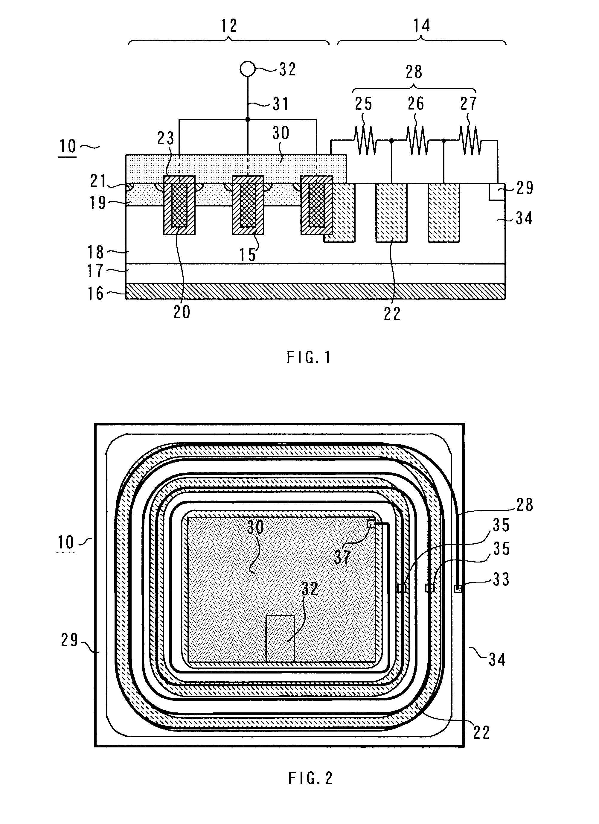
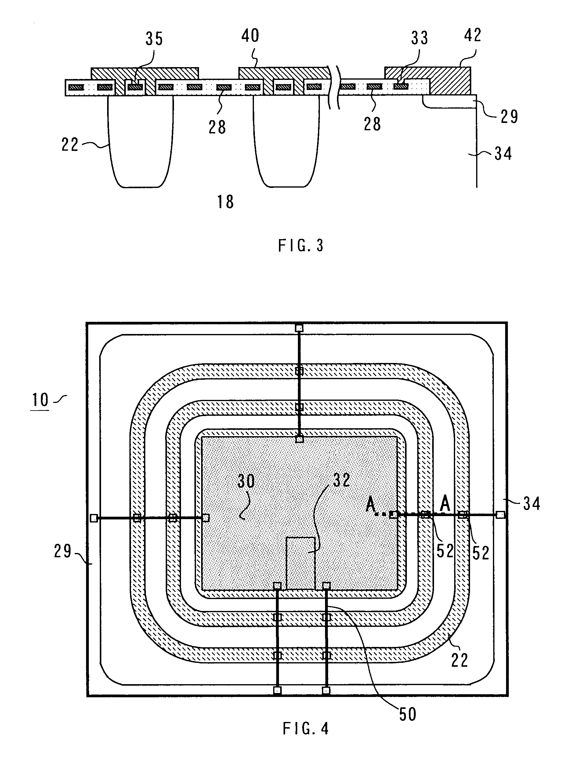
[0048]A first embodiment of the present invention relates to a semiconductor device with guard rings formed therein. This embodiment will be described in detail with reference to FIGS. 1 to 6. FIG. 6 is a cross-sectional view with a partial schematic, showing a semiconductor device 10 of the present embodiment. This semiconductor device 10 is formed from a single semiconductor substrate or chip, and includes a device region 12 in which a power device is formed, and a dielectric strength enhancing region 14 located around the device region 12. According to the present embodiment, the power device is a vertical IGBT which includes a plurality of integrated cells. In this example, the IGBT cells are of a trench type. However, they may be of a planar type.

[0049]The device region 12 and the dielectric strength enhancing region 14 are formed in the same semiconductor layer 18, which is an n layer. When the IGBT in the device region 12 is turned on, the semiconductor layer 18 receives carr...

second embodiment

[0068]A second embodiment of the present invention relates to a semiconductor device having a lateral MOSFET (a power device) therein. This embodiment will be described in detail with reference to FIGS. 8 to 11. FIG. 8 is a cross-sectional view with a partial schematic, showing a semiconductor device 70 of the present embodiment. This semiconductor device 70, which includes a lateral MOSFET, is formed from a semiconductor substrate and includes a semiconductor layer 72. The semiconductor layer 72 is an n− layer and has an n+ drain 74 formed in its surface. A drain electrode 76 of aluminum, etc. covers and is in electrical contact with the drain 74. Further, a p-base region 80 is formed in the surface of the semiconductor layer 72 and spaced from the n+ drain 74. An n+ source 91 and a p+ region 93 are formed in the surface of the p-base region 80, and a grounded source electrode 78 of aluminum, etc. covers and is in electrical contact with the source 91 and the p+ region 93.

[0069]An ...

third embodiment

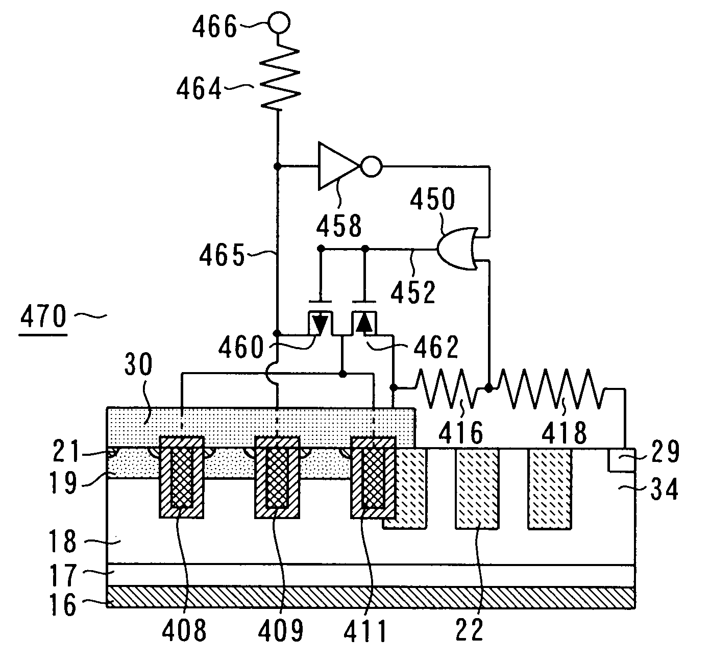
[0076]A third embodiment of the present invention relates to a semiconductor device that includes means for reducing the electric field in its semiconductor layer. This embodiment will be described with reference to FIG. 12. FIG. 12 is a cross-sectional view with a partial schematic, showing a semiconductor device 110 of the present embodiment. This semiconductor device 110 differs from the semiconductor device 70 of the second embodiment shown in FIG. 8 in the following respects.

[0077]The semiconductor device 110 includes a burying insulating film 112 which is formed within the semiconductor layer 72 and spaced from the top and bottom surfaces of the semiconductor layer 72. The burying insulating film 112 has a plurality of intra-insulating film electrodes 114 formed therein. The semiconductor device also includes a resistance element 120 which is capacitively coupled at one end to the drain 74 and at the other end to the p-base region 80, as respectively represented by a capacitor...


PUM


Abstract

A semiconductor device includes a semiconductor substrate including a semiconductor layer, a power device formed in the semiconductor substrate, a plurality of concentric guard rings formed in the semiconductor substrate and surrounding the power device, and voltage applying means for applying successively higher voltages respectively to the plurality of concentric guard rings, with the outermost concentric guard ring having the highest voltage applied thereto.

Description

BACKGROUND OF THE INVENTION[0001]1. Field of the Invention[0002]The present invention relates to semiconductor devices having therein a power semiconductor device such as an IGBT (Insulated Gate Bipolar Transistor) or a power MOSFET, and more particularly to such semiconductor devices with enhanced dielectric strength and short circuit protection capability.[0003]2. Background Art[0004]Enhanced dielectric strength and short circuit protection capability are required of semiconductor devices incorporating a power semiconductor device (or simply “power device”) which has a high voltage applied between its main electrodes. More specifically, such semiconductor devices must have a high dielectric strength and sufficient short circuit capability such that even if the load circuit connected between the main electrodes is short circuited, the power device does not degrade within a specified time period.[0005]It is common for these semiconductor devices to include structures such as guard r...

Claims


Application Information

Patent Timeline
Patent Type & Authority Applications(United States)
IPC IPC(8): H02H9/04H01L27/088
CPCH01L21/823814H01L21/823878H01L2924/0002H01L27/0921H01L28/20H01L29/0619H01L29/0638H01L29/0696H01L29/404H01L29/405H01L29/407H01L29/7397H01L29/7817H01L29/7824H03K17/08H01L29/7396H01L2924/00
Inventor KUSUNOKI, SHIGERU
Owner MITSUBISHI ELECTRIC CORP
Why Eureka
Try Eureka