Magnetic memory device

a memory device and magnetic technology, applied in the field of magnetic memory devices, can solve the problems of inability to reduce the layout area of memory cell arrays, the resistance of each source line is reduced, and the area of each mram cell is also increased, so as to reduce the resistance of each source line, the effect of efficiently disposing the piling region of word lines and reducing the resistan

Inactive Publication Date: 2010-05-13
RENESAS ELECTRONICS CORP
View PDF7 Cites 34 Cited by
  • Summary
  • Abstract
  • Description
  • Claims
  • Application Information

AI Technical Summary

Benefits of technology

[0025]Spaces along a row direction between first impurity regions are made different from each other thereby to make it possible to dispose piling regions for word lines efficiently and sufficiently ensure the distance between each of contacts for the piling regions and each of contacts for the first impurity regions. Thus, the word line piling regions are disposed with sufficient margins to thereby make it possible to realize a word line piling structure. Since the layout area of each memory cell does not increase, each word line can be brought to a reduction in the resistance sufficiently without increasing the area occupied by a memory cell array. Source wirings can be disposed in a column direction with sufficient widths. Thus, mesh-structured source lines can be realized and the resistance of each source...

Problems solved by technology

Therefore, if the word line piling structure of the DRAM is applied to the MRAM as it is, it is then difficult to reduce the layout area of a memory cell array.
A problem arises in that when the wi...

Method used


Image

  • Magnetic memory device
  • Magnetic memory device
  • Magnetic memory device

Examples


first embodiment

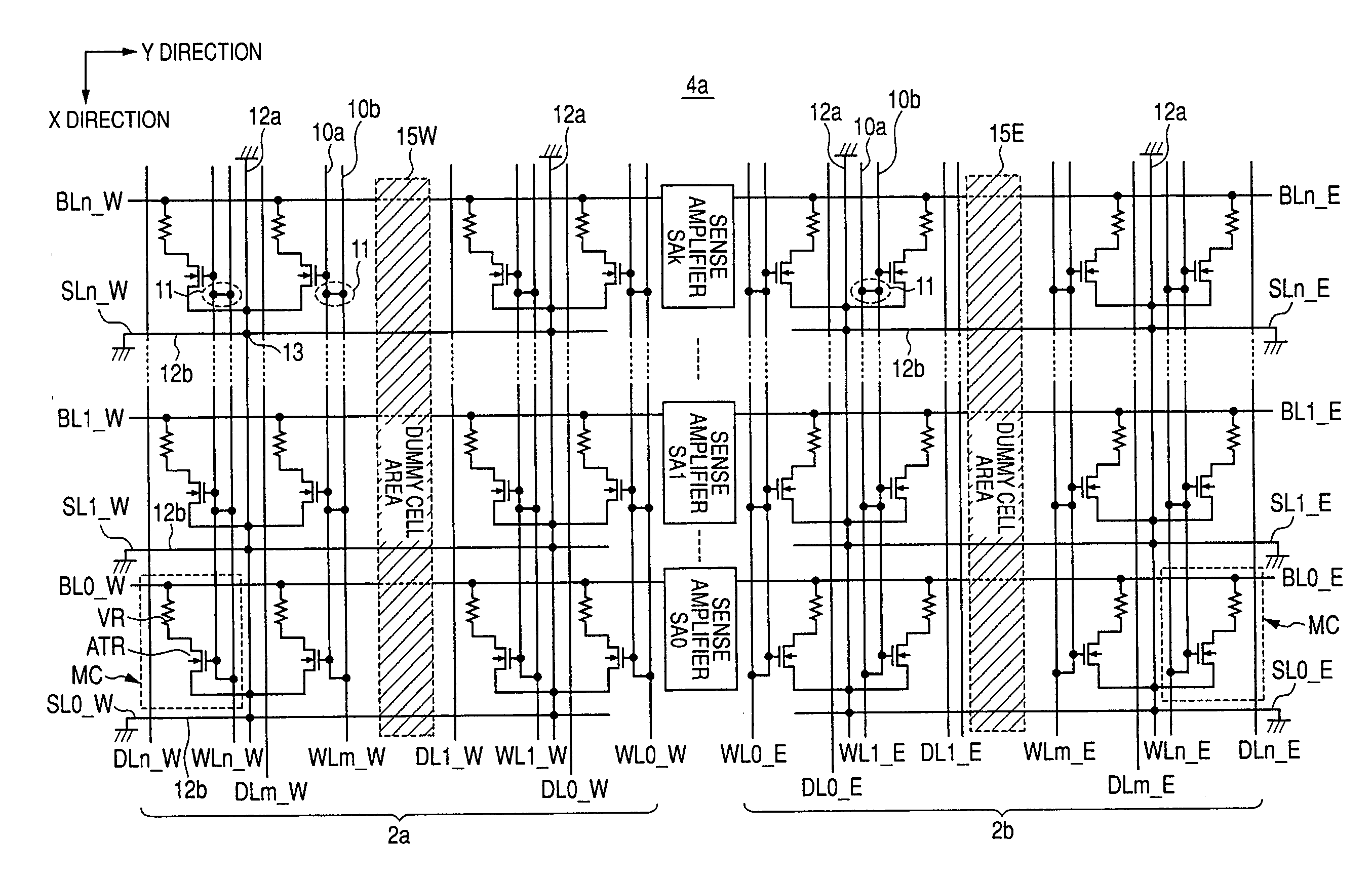
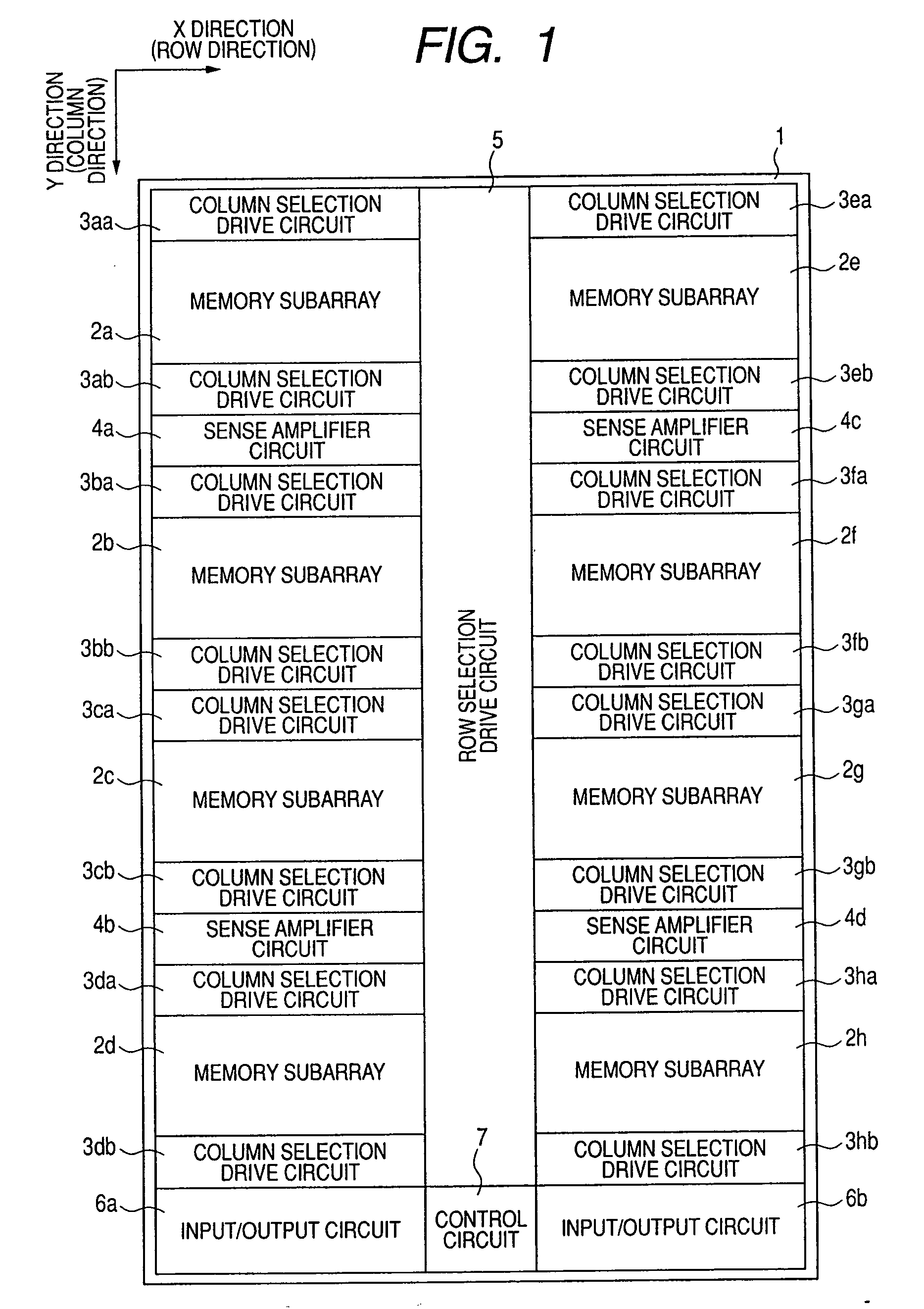
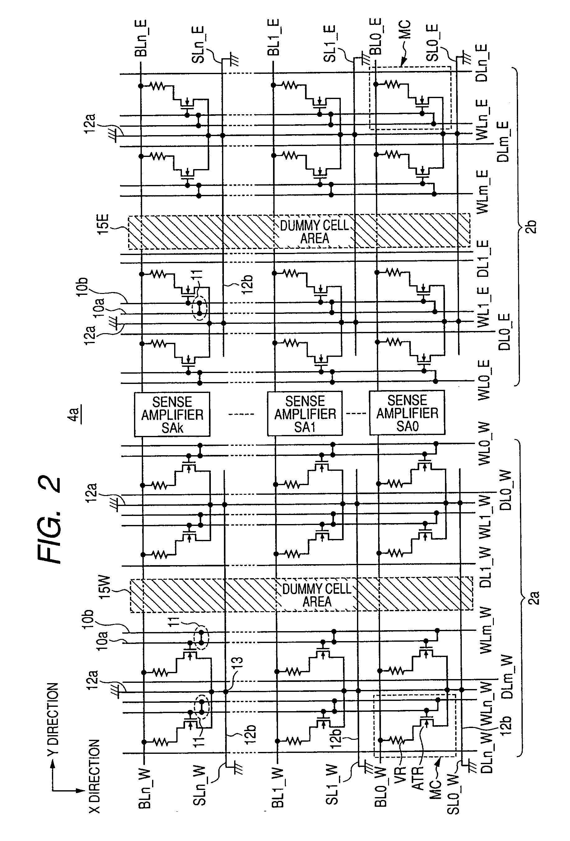
[0059]FIG. 1 is a diagram schematically showing an overall configuration of a non-volatile semiconductor memory device (MRAM) according to a first embodiment of the present invention. In FIG. 1, the non-volatile semiconductor memory device (hereinafter called “MRAM”) 1 is formed over a semiconductor chip (substrate) and includes a plurality of memory subarrays 2a through 2h. The memory subarrays 2a through 2h are arranged in line in a Y direction, and the memory subarrays 2e through 2h are arranged in line along the Y direction. In these memory subarrays 2a through 2h, MRAM cells are arranged in matrix form.

[0060]Column selection drive circuits 3aa, 3ab through 3ha and 3hb are provided on both sides extending along the Y direction, of the memory subarrays 2a through 2h respectively. Each of the column selection drive circuits 3aa, 3ab through 3ha and 3hb includes a column decoder which generates a column selection signal for selecting a column in accordance with an address signal, a...

second embodiment

[0176]FIG. 25 is a diagram schematically showing a fragmentary configuration of an MRAM according to a second embodiment of the present invention. A mode of coupling of MRAM cells to a sense amplifier where at memory subarrays 2a and 2b, memory cells of the memory subarray 2a are selected is schematically shown in FIG. 25. At the memory subarray 2a, memory cells MCa and MCb are coupled to a bit line BLaW. These memory cells MCa and MCb are different in position within the memory subarray 2a. Gates of corresponding access transistors ATR are coupled to their corresponding word lines WLaW and WLbW.

[0177]The bit line BLaW is coupled to its corresponding sense amplifier SA0 upon data reading. At the memory cell MCa, a variable magnetoresistive element VR and an access transistor ATR are interconnected with each other by means of an internal wiring LNa (intermediate wiring 40: any of 40a through 40d). At the memory cell MCb, a variable magnetoresistive element VR and an access transistor...

third embodiment

[0195]FIG. 28 is a diagram schematically showing a distribution of an initial resistance value of each variable magnetoresistive element at one memory subarray 2. In FIG. 28, the initial resistance value Rm of the variable magnetoresistive element easily increases from the center 0 of the memory subarray 2 to its ends (Lx and −Lx) in the X direction and becomes the highest at its peripheral portion. Similarly, as the distance from the center increases from the center (0) of the memory subarray 2 to its ends +Ly and −Ly in the Y direction, the initial resistance value Rm increases.

[0196]At each MRAM cell, a variable magnetoresistive element is formed by a ferromagnetic body and a barrier layer lying therebetween. The resistance value of the variable magnetoresistive element exponentially increases in accordance with the film thickness of the barrier layer. It is thus necessary to couple the barrier layer as thinly as possible. There is a need to accurately determine the composition a...


PUM


Abstract

The present invention provides a magnetic memory device capable of providing high-speed access without increasing an array area. Gate word lines are respectively linearly disposed between source impurity regions and drain impurity regions within a memory cell array area. Gate word line protrusions are respectively provided at boundary regions of memory cell forming regions. Contacts relative to the gate word line protrusions are respectively provided at boundary regions of memory cells at adjacent columns. The drain impurity regions are respectively disposed with being shifted from the centers of the memory cell forming regions in such a manner that spaces between the drain impurity regions become large in the regions in which the protrusions are disposed.

Description

CROSS-REFERENCE TO RELATED APPLICATIONS[0001]The disclosure of Japanese Patent Application No. 2008-291250 filed on Nov. 13, 2008 including the specification, drawings and abstract is incorporated herein by reference in its entirety.BACKGROUND OF THE INVENTION[0002]The present invention relates to a magnetic memory device, and particularly to a configuration of an array of a magnetic memory device capable of implementing high-speed access without increasing an area occupied by a memory cell array.[0003]As one of memory devices that store data therein on a non-volatile basis, there is known an MRAM (magnetic random access memory). The MRAM makes use of a variable magnetoresistive element for data storage. The variable magnetoresistive element has a TMR (tunneling magnetoresistive) element or an MTJ (magnetic tunneling junction) element. In either configuration, the variable magnetoresistive element has a fixed layer in which its direction of magnetization is fixed regardless of store...

Claims


Application Information

Patent Timeline
IPC IPC(8): G11C11/02G11C5/02
CPCG11C11/16G11C5/025G11C11/1659G11C11/1657G11C11/1673G11C11/1653
Inventor OKAYAMA, SHOTA
Owner RENESAS ELECTRONICS CORP
Why Eureka
Try Eureka