Semicondutor manufacturing method

a manufacturing method and semiconductor technology, applied in the direction of manufacturing tools, laser beam welding apparatus, welding/soldering/cutting articles, etc., can solve the problems of deterioration of semiconductors, reliability degradation, efficiency degradation of optical semiconductor devices, etc., to reduce production yield and chip yield

Inactive Publication Date: 2010-05-13
STANLEY ELECTRIC CO LTD
View PDF21 Cites 53 Cited by
  • Summary
  • Abstract
  • Description
  • Claims
  • Application Information

AI Technical Summary

Benefits of technology

[0011]The present invention was made in view of the above mentioned points. An object of the present invention is to provide a manufacturing method for semiconductor devices

Problems solved by technology

However, along the increase in the output power, the amount of heat generated by the optical semiconductor device has increased, which has caused a problem of reliability degradation such as efficiency degradation of an optical semiconductor device and deterioration of a semiconductor film.
The reason why such a method is used is because it is difficult to divide a wafer stably by using other methods and the difficulty of the dividing affects the yield.
For example, in a dicing method, due to the ductibility of the metal which constitutes the support, clogging of a dicing blade often occurs, and a blade needs to be replaced a number of times during the dicing process of the semiconductor device, which leads to a decrease of the work efficiency and an increase in the production cost.
On the other hand, in a scribing/breaking method, there is a problem in that the wafer is only bent due to the ductibility of the metal, and a wafer cannot be divided.
In these dicing method and scribing/breaking method, the thicker the metal support is, the more significant the above mentioned problem becomes.[Patent Document 1] Japanese Laid-Open Patent Application Publication No. 2007-536725.
However, even when a semiconductor device having a metal support is separated by using the laser scribing method, there have been the following problems.
However, the device separation may not properly occur, if a molten metal caused by the irradiation of the laser is not completely removed and remains inside the dividing groove, causing welding of the metal support again in the dividing groove. FIG. 1 is a cross-sectional photograph of a metal support in which a divi

Method used


Image

  • Semicondutor manufacturing method
  • Semicondutor manufacturing method
  • Semicondutor manufacturing method

Examples


first embodiment

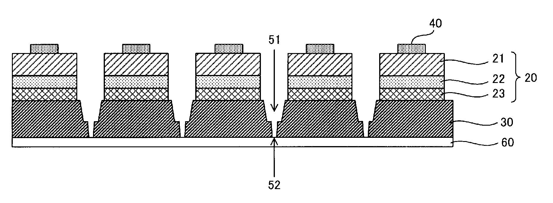
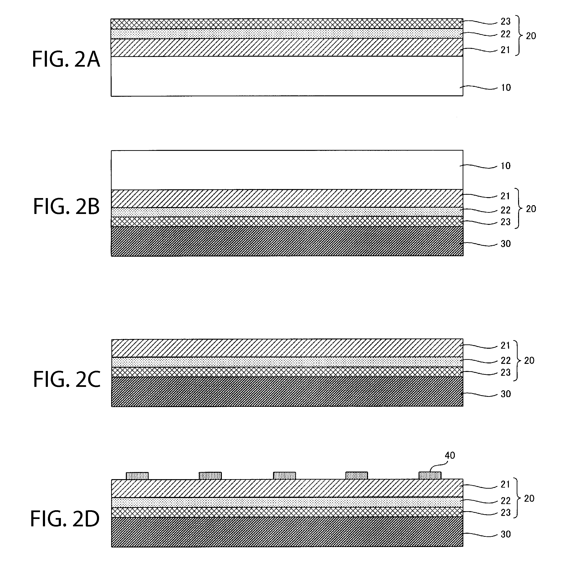
[0027]FIGS. 2A-2D and FIGS. 3E-3G are cross-sectional figures showing a manufacturing method of optical semiconductor devices according to a first embodiment of the present invention. FIG. 4 is a flow chart showing a manufacturing method of optical semiconductor devices according to the first embodiment of the present invention.

[0028](Semiconductor Layer Growth Step; Step S10) A growth substrate is prepared. In the present embodiment, a C-plane sapphire substrate 10 is used as a growth substrate because a semiconductor film made of AlxInyGazN (0≦x≦1, 0≦y≦1, 0≦z≦1, x+y+z=1) can be formed thereon using the MOCVD method (metal organic chemical vapor deposition method). Each of the layers that constitute the semiconductor layer 20 is laminated on the sapphire substrate 10 along the C-axis direction of the wurtzite-type crystal structure by using the MOCVD method.

[0029]First, the thermal cleaning of the sapphire substrate 10 is performed. Specifically, the sapphire substrate 10 is introd...

second embodiment

[0056]In the following, a second embodiment according to the present invention is described. In the present embodiment, the processes, which were described above with reference to FIGS. 2A-2E, are the same as those in the first embodiment, but only the step S60 (the dividing process of devices) which was described above with reference to FIGS. 3E-3G is different from that in the first embodiment. However, in this example, the thickness of the metal support 30 was set to 120 μm. Other differences are explained with reference to FIGS. 7E-7G.

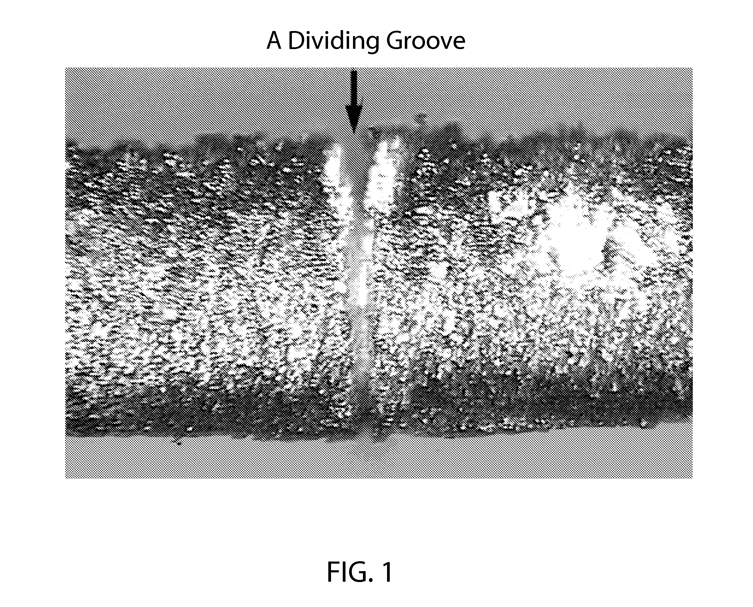
[0057](Device Dividing Step; Step S60) Along the street groove 50 formed on the semiconductor film 20, the metal support 30 is cut by using a laser scribing method using YAG crystal (Yttruim•Aluminium•Garnet) as a laser medium, for example, to separate the semiconductor devices. In the present embodiment, dividing of the devices is done by using two stages of the laser beam radiation (steps S61, S62) having different conditions for the laser beam r...


PUM

PropertyMeasurementUnit
Thicknessaaaaaaaaaa
Thicknessaaaaaaaaaa
Thicknessaaaaaaaaaa

Abstract

A manufacturing method for semiconductor devices having a metal support is provided. The method in one aspect includes growing a semiconductor film on a growth substrate; forming a metal support on a surface of said semiconductor film opposite to the growth substrate; thereafter removing said growth substrate from said semiconductor film; forming a street groove reaching said metal support in the said semiconductor film; radiating a first laser beam onto said metal support to form a first dividing groove having a substantially flat bottom in said metal support; and radiating a second laser beam onto said metal support to form a second dividing groove that penetrates though a portion of said metal support that remains where the first divining groove is formed.

Description

BACKGROUND[0001]1. Technical Field[0002]The present invention relates to a manufacturing method of a semiconductor device. More specifically, the present invention relates to a dicing technique of a semiconductor device having a metal support by using a laser scribing method.[0003]2. Related Art[0004]Owing to the technological progress of recent years, optical semiconductor devices, such as a light emitting diode, have achieved a higher efficiency and higher output powers. However, along the increase in the output power, the amount of heat generated by the optical semiconductor device has increased, which has caused a problem of reliability degradation such as efficiency degradation of an optical semiconductor device and deterioration of a semiconductor film. In order to solve these problems, the growth substrate that typically has a relatively low thermal conductance has been discarded and replaced with a structure in which a metal support having a relatively high thermal conductan...

Claims


Application Information

Patent Timeline
IPC IPC(8): H01L21/78H01L21/302
CPCB23K26/0604H01L33/0095B23K26/409B23K26/367Y10S438/977B23K26/364B23K26/40B23K2103/172
Inventor SAITO, TATSUMATANAKA, SHINICHIYOKOBAYASHI, YUSUKE
Owner STANLEY ELECTRIC CO LTD
Why Eureka
Try Eureka