Liquid crystal display device

a display device and liquid crystal technology, applied in the field of semiconductor devices, can solve the problems of easy deterioration of transistors and malfunctions of circuits, and achieve the effect of suppressing deterioration of transistors and improving reliability of circuits including transistors

Active Publication Date: 2010-05-20
SEMICON ENERGY LAB CO LTD
View PDF7 Cites 47 Cited by
  • Summary
  • Abstract
  • Description
  • Claims
  • Application Information

AI Technical Summary

Benefits of technology

[0068]According to one embodiment of the invention disclosed in this specification, deterioration in a transistor can be suppressed.
[0069]Alternatively, according to one embodiment of the invention disclosed in this specification, a malfunction of a circuit due to deterioration in a transistor can be suppressed.
[0070]Alternatively, according to one embodiment of the invention disclosed in this specification, reliability of a circuit including a transistor can be improved.

Problems solved by technology

In the case where the transistor deteriorates, for example, there is a problem in that a shift in threshold voltage, where the threshold voltage is shifted positively, occurs and that a malfunction of a circuit occurs.
That is, since a source and a drain of a transistor are fixed, an electric field concentrates on a drain side and the transistor easily deteriorates.

Method used


Image

  • Liquid crystal display device
  • Liquid crystal display device
  • Liquid crystal display device

Examples


embodiment 1

[0109]In this embodiment, examples of a semiconductor device including a transistor are described.

[0110]In order to suppress deterioration in a transistor, in the semiconductor device described in this embodiment, the direction of current flowing through the transistor is changed (inverted) in a period during which the transistor is on. That is, by changing the level of voltage applied to a first terminal and a second terminal (terminals serving as a source and a drain) of the transistor in the period during which the transistor is on every given period, the source and the drain are switched every given period. Specific circuit structures and operation are described below with reference to drawings.

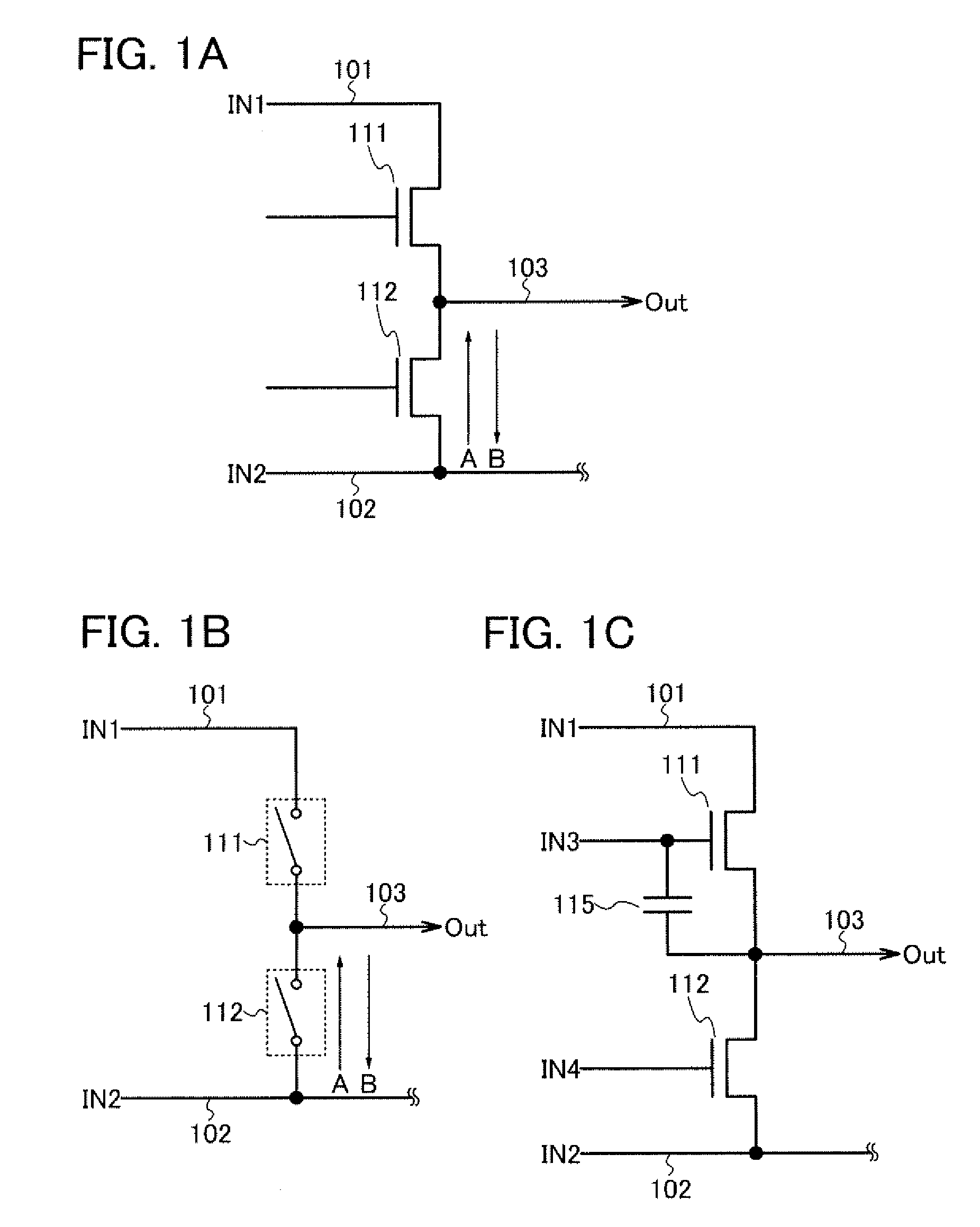
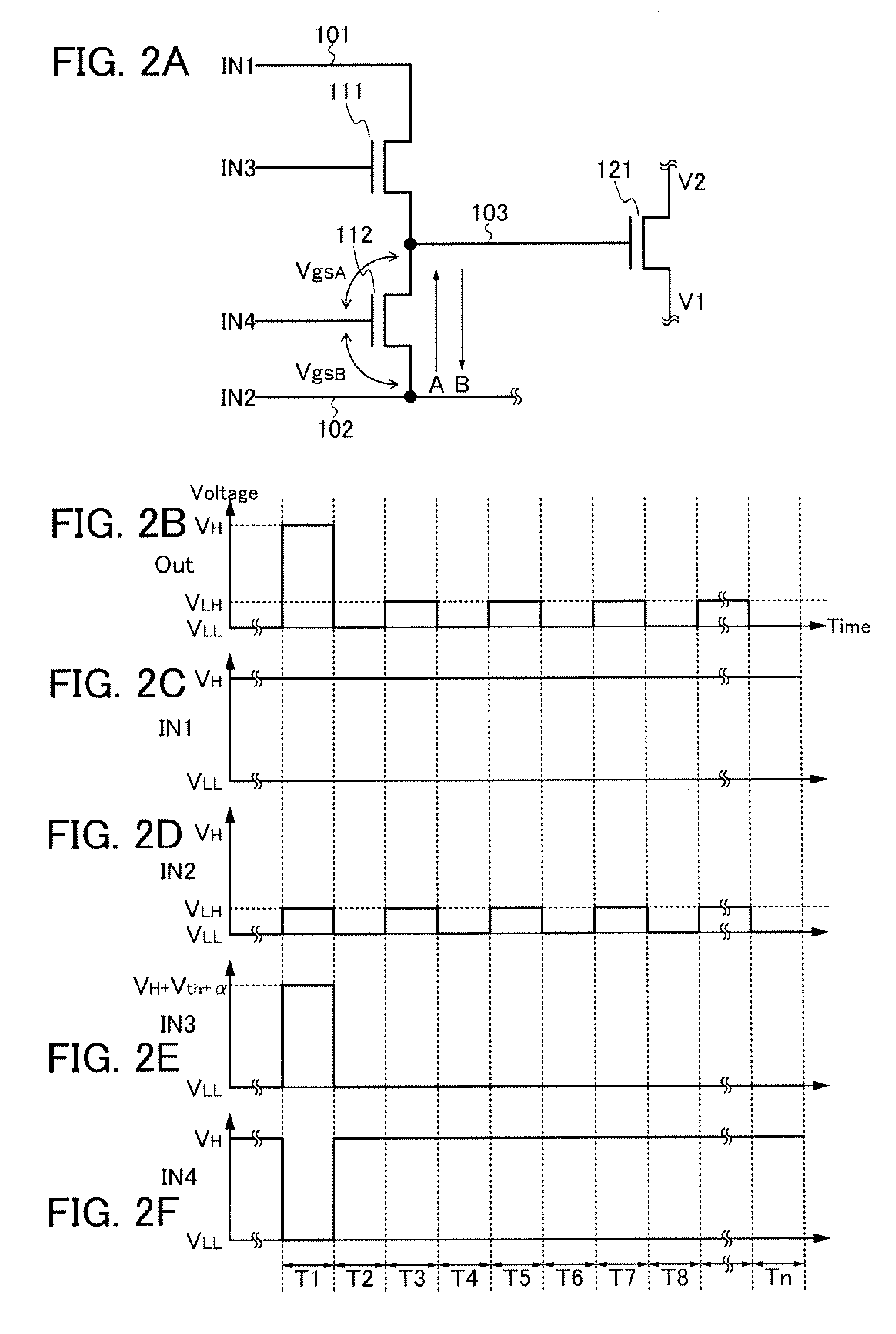
[0111]The semiconductor device described in this embodiment includes at least a transistor 111 provided between a wiring 101 and a wiring 103 and a transistor 112 provided between a wiring 102 and the wiring 103 (see FIG. 1A).

[0112]One of a source and a drain of the transistor 111 is elec...

embodiment 2

[0146]In this embodiment, examples of a semiconductor device having a structure which is different from the structure in the above embodiment are described with reference to drawings.

[0147]The semiconductor device described in this embodiment includes at least the transistor 111 provided between the wiring 101 and the wiring 103 and a plurality of transistors 112a and 112b provided in parallel with each other between the wiring 102 and the wiring 103 (see FIG. 5A). That is, the structure illustrated in FIG. 5A is a structure obtained by adding the transistor 112b to the structure illustrated in FIG. 1A (the transistor 112a in FIGS. 5A to 5C corresponds to the transistor 112 in FIGS. 1A to 1C). Note that although FIG. 5A illustrates the case where two transistors (the transistors 112a and 112b) are provided in parallel, three or more transistors may be provided.

[0148]One of a source and a drain of each of the transistors 112a and 112b is electrically connected to the wiring 102, and ...

embodiment 3

[0210]In this embodiment, examples of a semiconductor device having a structure which is different from the structure in the above embodiment are described with reference to drawings.

[0211]The semiconductor device described in this embodiment includes at least the transistor 111 provided between the wiring 101 and the wiring 103, the transistor 112 provided between the wiring 102 and the wiring 103, and a transistor 114 provided between a wiring 104 and the wiring 103 (see FIG. 12A).

[0212]One of a source and a drain of the transistor 114 is electrically connected to the wiring 104, and the other of the source and the drain of the transistor 114 is electrically connected to the wiring 103. That is, the structures illustrated in FIGS. 12A to 12C are structures obtained by adding the wiring 104 to the structures illustrated in FIGS. 5A to 5C and by electrically connecting the one of the source and the drain of the transistor 112b in FIGS. 5A to 5C not to the wiring 102 but to the wirin...


PUM

PropertyMeasurementUnit
currentaaaaaaaaaa
currentaaaaaaaaaa
threshold voltageaaaaaaaaaa

Abstract

To suppress a malfunction of a circuit due to deterioration in a transistor. In a transistor which continuously outputs signals having certain levels (e.g., L-level signals) in a pixel or a circuit, the direction of current flowing through the transistor is changed (inverted). That is, by changing the level of voltage applied to a first terminal and a second terminal (terminals serving as a source and a drain) every given period, the source and the drain are switched every given period. Specifically, in a portion which successively outputs signals having certain levels (e.g., L-level signals) in a circuit including a transistor, L-level signals having a plurality of different potentials (L-level signals whose potentials are changed every given period) are used as the signals having certain levels.

Description

BACKGROUND OF THE INVENTION[0001]1. Field of the Invention[0002]The present invention relates to semiconductor devices. In particular, the present invention relates to semiconductor devices formed using transistors and an operating method thereof. Further, the present invention relates to display devices including semiconductor devices and electronic devices including the display devices.[0003]2. Description of the Related Art[0004]In recent years, display devices such as liquid crystal display devices and light-emitting devices have actively developed. In particular, a technique for forming a pixel circuit and a driver circuit including a shift register circuit or the like (hereinafter referred to as an internal circuit) over the same insulator by using transistors formed using a non-single-crystal semiconductor has actively developed, because the technique greatly contributes to reduction in power consumption and cost, improvement in reliability, and decrease in frame. The interna...

Claims


Application Information

Patent Timeline
Patent Type & Authority Applications(United States)
IPC IPC(8): G09G3/36G02F1/1368
CPCG09G3/20G09G3/3233G09G3/3677G09G2300/0408G09G2300/0417G09G2300/0847G11C19/28G09G2310/0267G09G2310/0286G09G2310/0291G09G2310/08G09G2320/043G09G2310/0254G09G3/3648G09G2300/0426G02F1/133638H10K10/482H10K10/20G02F1/133528G02F1/136286
Inventor KIMURA, HAJIME
Owner SEMICON ENERGY LAB CO LTD
Why Eureka
Try Eureka