Semiconductor memory device and control method thereof

a memory device and semiconductor technology, applied in the direction of information storage, static storage, digital storage, etc., can solve the problems of inability to have compatibility, difficult to determine the data held by the phase change memory cell, and difficulty in achieving high speed access, so as to achieve high speed, reduce consumption power, and not shorten the life of the memory cell

Inactive Publication Date: 2010-05-20
ELPIDA MEMORY INC
View PDF2 Cites 45 Cited by
  • Summary
  • Abstract
  • Description
  • Claims
  • Application Information

AI Technical Summary

Benefits of technology

[0012]According to the present invention, each sense amplifier is connected through two data lines to an input / output circuit. Accordingly, a pre-write operation and an actual write operation according to write data can be performed at high speed. Further, because only memory cells selected by a column address are subjected to write, consumption power is reduced and lives of memory cells are not shortened.
[0013]As the present invention is applied to an ordinary PRAM that stores one bit of data in one phase change memory cell while ensuring high speed access, an intermediate state of a phase change material can be properly eliminated. As the present invention is applied to a multi-bit PRAM that stores two or more bits of data in one phase change memory cell, accurate control can be realized so that the phase change material is in a desired intermediate state.

Problems solved by technology

In this case, data held by the phase change memory cell is difficult to be determined, and this can be a cause of errors.
Accordingly, high speed access becomes difficult to achieve, and the PRAM in this case cannot have a compatibility with a DRAM (Dynamic Random Access Memory), for example.
However, because the PRAM described in Japanese Patent Application Laid-open No. 2006-302465 performs a set operation (a pre-write operation) upon all memory cells corresponding to the selected word line, power consumption therefore is increased.
Also in a reset operation in response to a PRE command, when the number of memory cells to be reset is large, the power consumption is increased accordingly.
Further, as the pre-write operation is performed in response to an ACT command, the pre-write operation and the write operation are performed during a read operation, and this causes the life of the memory cell to be shortened.

Method used


Image

  • Semiconductor memory device and control method thereof
  • Semiconductor memory device and control method thereof
  • Semiconductor memory device and control method thereof

Examples


first embodiment

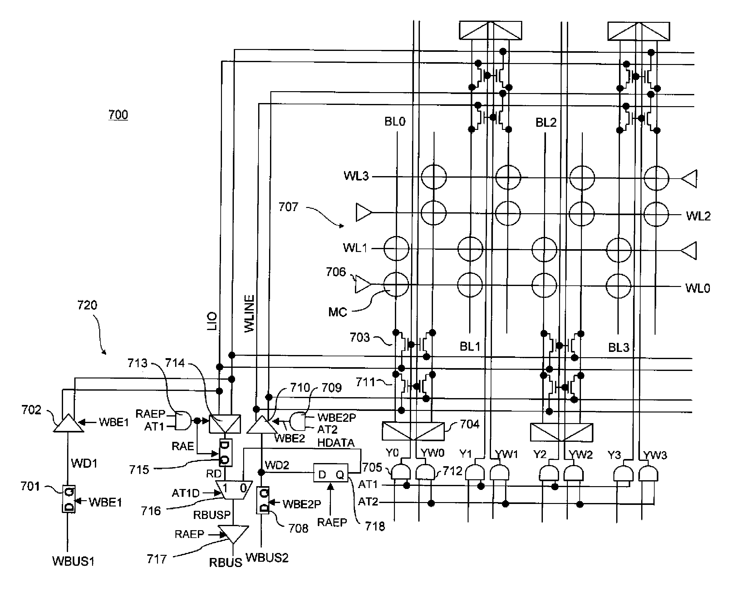
[0038]FIG. 1 is a circuit diagram showing a configuration of principal parts of a semiconductor memory device 700 according to the

[0039]As shown in FIG. 1, the semiconductor memory device 700 according to the first embodiment includes a phase-change memory cell array 707 that includes the word lines WL0, WL1, . . . , the bit line pairs BL0, BL1, . . . , and the memory cells MC arranged at intersections of the word lines with the bit lines. Sense amplifiers 704 are connected to each of the bit line pairs BL0, BL1, . . . . Each of the sense amplifiers 704 is connected via a corresponding column switch 703 to the I / O line LIO and via a corresponding column switch 711 to the data line WLINE for write. Column select signals Y0, Y1, . . . serving as outputs of column select drivers 705 are supplied to the respective column switches 703 and any one of the switches is turned on during the read operation or the write operation. Meanwhile, column select signals YW0, YW1, . . . for write servi...

second embodiment

[0075]the present invention is described next.

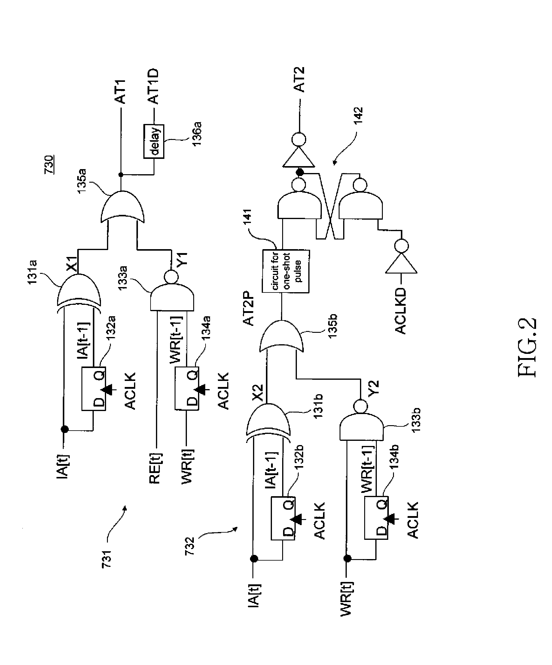
[0076]While the first embodiment performs the write operation promptly after the pre-write operation in the write cycle, the second embodiment performs the write operation and the pre-write operation in synchronization with the clock. Because the clock ACLKD estimating the pre-write operation time does not exist, the address transition detection signal AT2 for the write-to-write operation is generated by a detection circuit 730a shown in FIG. 6. The detection circuit 730a shown in FIG. 6 has a circuit configuration obtained by omitting SR-FF from the detection circuit 730 shown in FIG. 2. The circuit part that generates the address transition detection signal AT1 for the write-to-read operation is unchanged.

[0077]FIG. 7 is a timing diagram showing the write-to-write-to-read operation for the same address.

[0078]First, when the address corresponding to the bit line pair BL0 is specified and a write request is issued at the time t1, the pre...

third embodiment

[0086]the present invention is described next.

[0087]According to recent DRAMs, a predetermined latency can be added to the period from when a write command is inputted to when the write operation upon an array is started. For example, according to DDR DRAMs, DQS starts to be inputted in the current cycle, data is fetched in synchronization with DQS in the next cycle, and the data is provided in synchronization with CLK in the cycle after the next cycle. Two cycles of the latency are thus provided. When a calculation is completed within the two cycles and the write operation is performed in the regular latency, the spec tDPL(tWR) is not violated. The third embodiment provides an example applying the configuration described in the second embodiment one cycle earlier. “Earlier” means that, for the pre-write operation and the write operation in response to an issuance of a write request, the pre-write operation is performed during a write latency period and the write operation is perfor...


PUM


Abstract

To provide data lines connected via column switches to a plurality of sense amplifiers and an input/output circuit that, in response to a write request, supplies pre-write data through the data line to selected phase change memory cells and then write data through the data line to the selected phase change memory cells. Thus, a pre-write operation and an actual write operation according to the write data can be performed at high speed. Because only the memory cells selected by a column address are subject to write, consumption power is reduced and lives of the memory cells are not shortened.

Description

BACKGROUND OF THE INVENTION[0001]1. Field of the Invention[0002]The present invention relates to a semiconductor memory device and a control method thereof, and more particularly relates to a semiconductor memory device having phase change memory cells and a control method thereof.[0003]2. Description of Related Art[0004]Recently, PRAM (Phase change Random Access Memory) has attracted attention as a non-volatile memory that realizes high speed access. The PRAM is configured by phase change memory cells including phase change materials and holds information based on the difference of an electric resistance depending on a phase state of the phase change material. Specifically, when the phase change material is in a crystalline state (a set state), relatively low resistance is provided, and when the phase change material is in an amorphous state (a reset state), relatively high resistance is provided. Accordingly, when the phase change material is either in the crystalline state or in ...

Claims


Application Information

Patent Timeline
Patent Type & Authority Applications(United States)
IPC IPC(8): G11C11/00G11C5/02
CPCG11C11/56G11C11/5678G11C13/0004G11C13/0023G11C13/0026G11C2213/79G11C13/0069G11C2013/0076G11C2013/0078G11C2013/0092G11C2207/002G11C13/0061
Inventor ARAI, TETSUYA
Owner ELPIDA MEMORY INC
Why Eureka
Try Eureka