White organic electroluminescent element and lighting device

Active Publication Date: 2010-05-27
MERCK PATENT GMBH
View PDF5 Cites 37 Cited by
  • Summary
  • Abstract
  • Description
  • Claims
  • Application Information

AI Technical Summary

Benefits of technology

[0032]The present invention has enabled to provide an organic electroluminescent element yielding white luminescence which is excellent in electric power efficiency, storage stability, color rendering prope

Problems solved by technology

An inorganic electroluminescent element has been utilized as a flat light source, however, it requires a high voltage of alternating current to operate an emission element.
On the other hand, in the case of a phosphorescence material which utilizes an emission from an excited triplet state, the upper limitation of the internal quantum efficiency will be 100% by considering the production ratio of excitons and internal conversion of a singlet exciton to a triplet exciton.
However, there has been developed no good phosphorescence emitting material which yields blue emission a

Method used


Image

  • White organic electroluminescent element and lighting device
  • White organic electroluminescent element and lighting device
  • White organic electroluminescent element and lighting device

Examples


example 1

Preparation of Organic EL Elements

[Preparation of Organic EL Element 1]

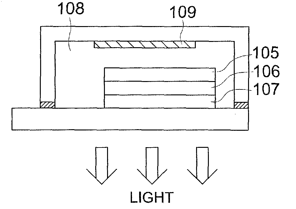
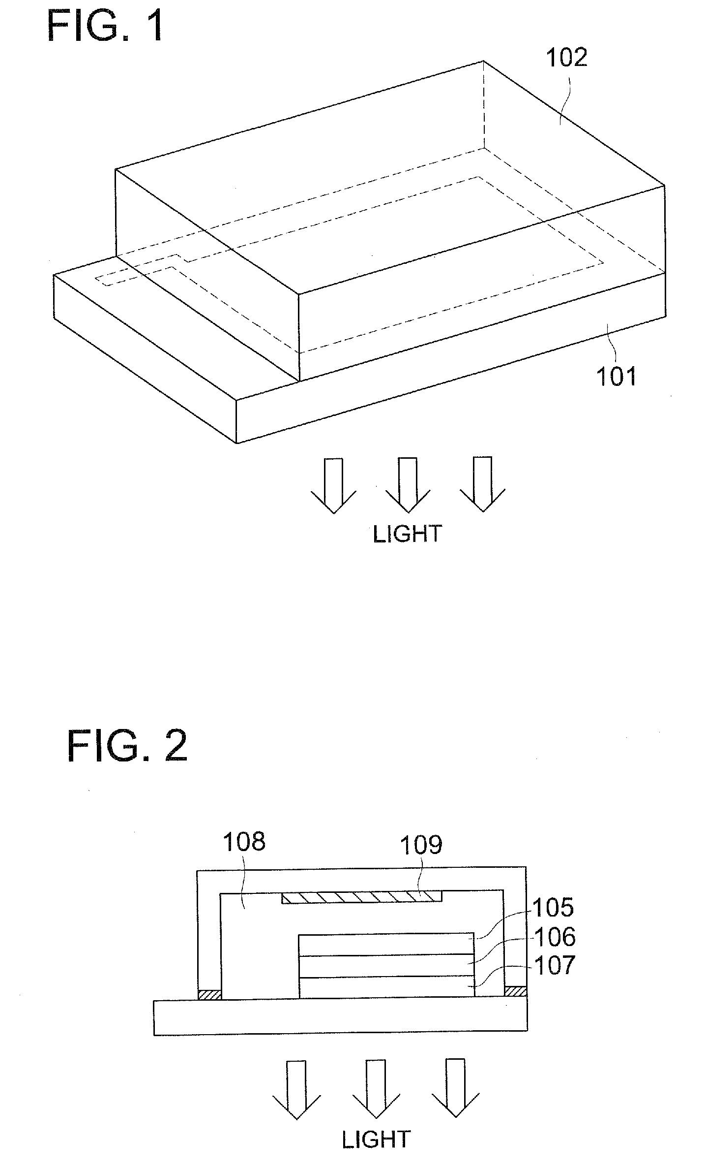
[0262]A 120 nm thick ITO (indium tin oxide) film was formed as an anode on a 0.7 mm thick 30 mm×30 mm glass substrate. The resulting substrate was subjected to patterning. Thereafter, the transparent substrate, fitted with the above ITO transparent electrode, was subjected to ultrasonic cleaning employing isopropyl alcohol, dried employing nitrogen gas, and subjected to UV ozone cleaning over 5 minutes. Thereafter, the resulting transparent substrate was fixed in the substrate holder in a commercial vacuum deposition apparatus. Each of the materials in an optimal amount constituting each layer was placed in each crucible for deposition in the vacuum deposition apparatus. The employed crucible for deposition was prepared via resistance heating materials such as molybdenum or tungsten.

[0263]After subjected to plasma treatment for 2 minutes at an oxygen gas pressure of 1 Pa and an electric power of 100 W (an area of...

example 2

Preparation of Organic EL Element

[Preparation of Organic EL Element 8]

[0294]Organic EL Element 8 was prepared in the same manner as used for the preparation of Organic EL Element 3, except that the layer thickness of the green-red phosphorescence emitting layer (Light Emitting Layer 1 in Example 1) and the host compound employed therein were changed to those described in Table 3. Then Lighting Device 8 was prepared using Organic EL Element 8 in the same manner as in Example 1.

TABLE 3OrganicPositive HolePositive HoleLight EmittingLight EmittingPositive HoleElectronELInjectionTransportLayer 1Layer 2InhibitionTransport LayerElementLayer (layerLayer (layerDopantDopantLayer (layerDopantNo.thickness nm)thickness nm)(weight %)*1(weight %)*1thickness nm)(weight *)*1Remarks8m-MTDATA(10)α-NPD(30)Ir-1(15)CBP(12)E-66(15→9)1-6(15)M-1(5)CsF(10)M-1(45)Inv.Ir-14(2)*1: Host compound (layer thickness nm),Inv.: Present Invention

[0295]The structure of the compound (CBP) listed in Table 3, but not liste...

example 3

Preparation of Organic EL Elements 9 to 11

[0298]Organic EL Elements 9 to 11 were prepared in the same manner as the preparation of Organic EL Element 3 described in Example 1, except that the host compound employed in the blue phosphorescence emitting layer (Light Emitting Layer 2 in Table 1) and the layer thickness thereof were changed to those described in Table 5, thereafter, Lighting Devices 9 to 11 were prepared in the same manner as in Example 1.

TABLE 5OrganicPositive HolePositive HoleLight EmittingLight EmittingPositive HoleElectronELInjectionTransportLayer 1Layer 2InhibitionTransport LayerElementLayer (layerLayer (layerDopantDopantLayer (layerDopantNo.thickness nm)thickness nm)(weight %)*1(weight %)*1thickness nm)(weight %)*1Remarks9m-MTDATA(10)α-NPD(30)Ir-1(15)1-6(8)E-66(15→9)1-10(14)M-1(5)CsF(10)M-1(45)Inv.Ir-14(2)10m-MTDATA(10)α-NPD(30)Ir-1(15)1-6(8)E-66(15→9)1-7(14)M-1(5)CsF(10)M-1(45)Inv.Ir-14(2)11m-MTDATA(10)α-NPD(30)Ir-1(15)1-6(8)E-66(15→9)1-31(12)M-1(5)CSF(10)M-1(45)...


PUM


Abstract

Disclosed is a white light-emitting organic electroluminescent device, which is excellent in stability of emission chromaticity over a long operation period, while having high electrical efficiency, long life, excellent storage stability and excellent color rendering properties. Also disclosed is an illuminating device using such an organic electroluminescent device. Specifically disclosed is an organic electroluminescent device having a light-emitting layer between an anode and a cathode, which is characterized by comprising a light-emitting layer A having a maximum emission wavelength of not more than 480 nm and containing a phosphorescent dopant having a maximum emission wavelength of not more than 480 nm, and a light-emitting layer B arranged between the light-emitting layer A and the anode, which has a maximum emission wavelength of not less than 510 nm and contains a phosphorescent dopant. This organic electroluminescent device is also characterized in that the concentration of the phosphorescent dopant contained in the light-emitting layer A varies in the thickness direction of the light-emitting layer A. Also specifically disclosed is an illuminating device using such a white light-emitting organic electroluminescent device.

Description

TECHNICAL FIELD[0001]The present invention relates to a white light emitting organic electroluminescent element which contains a plurality of light emitting materials having a different emission wavelength and includes a blue phosphorescence emitting material. The present invention also relates to a lighting device using the aforesaid white organic electroluminescent element.BACKGROUND ART[0002]An emission type electronic display device includes an electroluminescence display (hereinafter, referred to as an ELD). A constituent element of an ELD includes such as an inorganic electroluminescent element ((hereinafter, it is also referred to as an inorganic EL element) and an organic electroluminescent element (hereinafter, it is also referred to as an organic EL element). An inorganic electroluminescent element has been utilized as a flat light source, however, it requires a high voltage of alternating current to operate an emission element.[0003]On the other hand, an organic electrolu...

Claims


Application Information

Patent Timeline
IPC IPC(8): H01L51/54H01L51/52
CPCC09K11/06Y02B20/181C09K2211/1044C09K2211/1092C09K2211/185H01L51/0071H01L51/0072H01L51/0085H01L51/0086H01L51/0087H01L51/0088H01L51/5016H01L51/5036H05B33/14C09K2211/1029Y02B20/00H10K85/348H10K85/344H10K85/346H10K85/657H10K85/342H10K85/6572H10K50/125H10K50/11H10K2101/10
Inventor NAKAYAMA, YORIKONAKAYAMA, TOMOYUKIHIYAMA, KUNIMASAKOJIMA, SHIGERU
Owner MERCK PATENT GMBH
Why Eureka
Try Eureka