
Back-Contacted Photovoltaic Device

a photovoltaic cell and back contact technology, applied in the direction of photovoltaic energy generation, electrical equipment, basic electric elements, etc., can solve the problems of increasing the risk of a chip breaking in the final manufacturing stage the deterioration of the photovoltaic cell, and the crucial issue of the screen printing process, so as to increase the effective surface area and increase the temperature of the silicon. , the effect of high efficiency

Inactive Publication Date: 2010-06-03
XGROUP
View PDF6 Cites 0 Cited by
  • Summary
  • Abstract
  • Description
  • Claims
  • Application Information

AI Technical Summary

Benefits of technology

[0005]As concerns the emitter contacts, several currently known technologies are capable of producing highly efficient devices, in which the emitter contacts are positioned at the back of the photovoltaic device, thus maximizing the surface area available for solar energy conversion.
[0038]As for the manufacture of said diffuser elements using laser technology, it has been demonstrated that a suitable laser source is capable of locally increasing the temperature of the silicon until it becomes sublimated without excessively damaging the cross-linking of the crystals around the radiated area. It is consequently considered feasible to obtain suitably doped areas, such as those needed to realize the new device, by means of a diffusion of the impurities in the liquid phase, achieved by melting said areas with the aid of a laser. The object is to obtain diffuser elements as deep as the full thickness of the p-doped part by means of a rapid, reliable process, that can be done in milliseconds.

Problems solved by technology

As a result, there is currently a growing tendency to reduce the thickness of the wafers, but this has its drawbacks.
In fact, because of its reduced thickness, the aluminum paste deposited on the back of the device tends to bend the wafer and thus increases the risk of it breaking in the photovoltaic cell's final manufacturing stages.
The screen-printing process is consequently proving a crucial issue in terms of reducing the thickness of the wafers being used.
On the other hand, the previously-mentioned highly efficient processes have several drawbacks that, for various reasons, prevent them from gaining a dominant role on the market.
The efficiency of the known photovoltaic devices is also limited by the presence of the metal emitter contacts on the front surface, which act as a shield on the surface of the solar cell, thus reducing the active surface area of the device.
The efficiency of such devices is the highest available on the market, but the sophisticated steps involved in their manufacture and the special base materials needed (FZ Si) make the procedure rather complex and costly.

Method used


Image

  • Back-Contacted Photovoltaic Device
  • Back-Contacted Photovoltaic Device
  • Back-Contacted Photovoltaic Device

Examples


Embodiment Construction

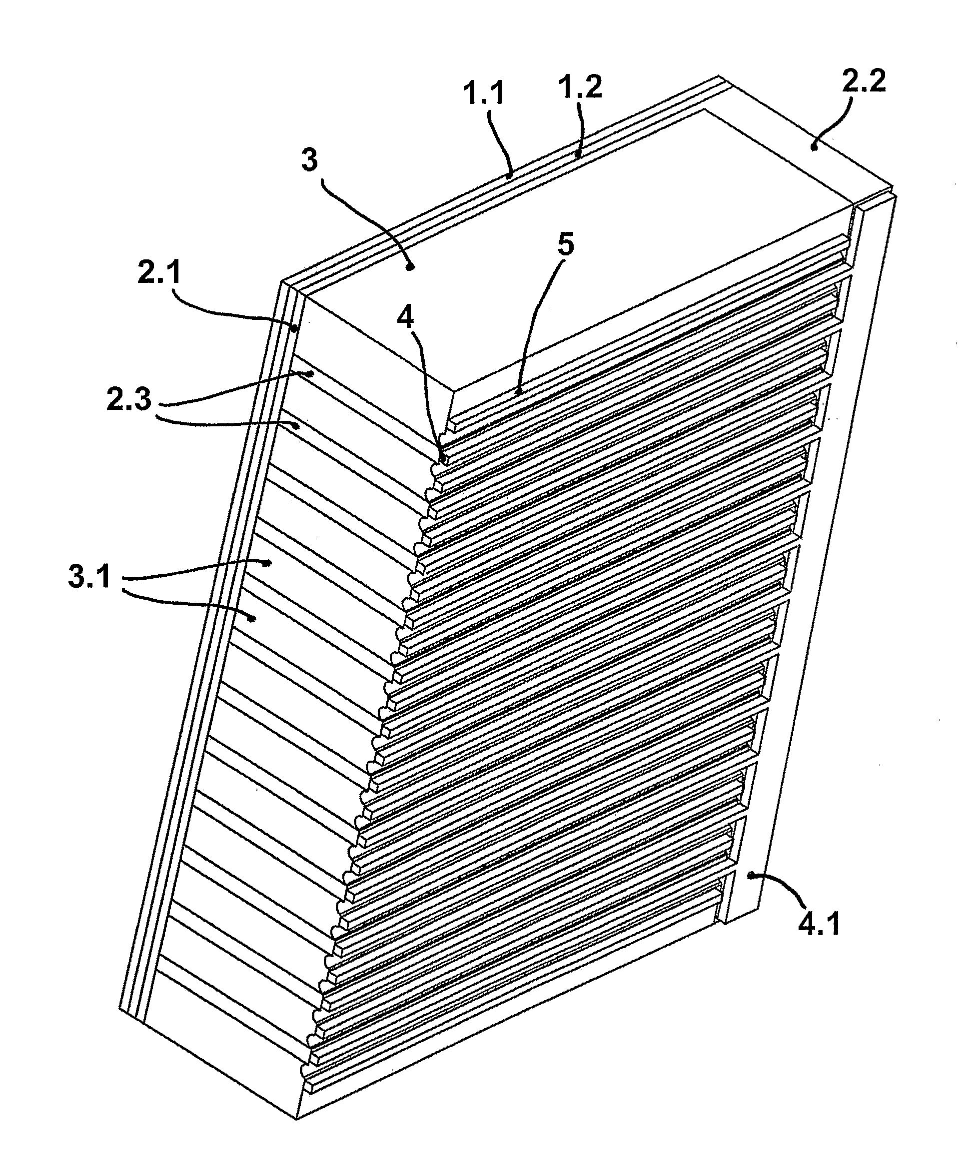
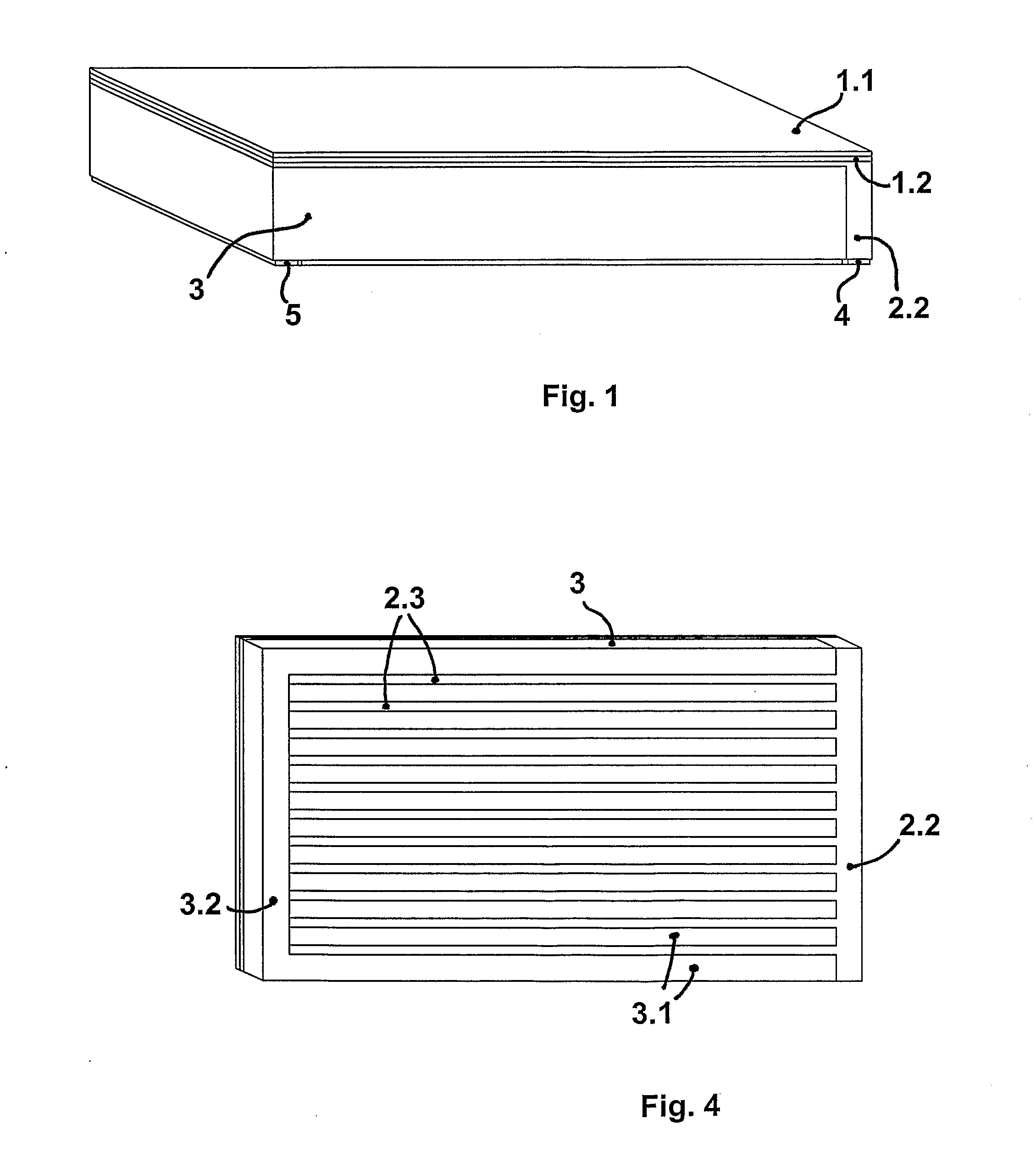
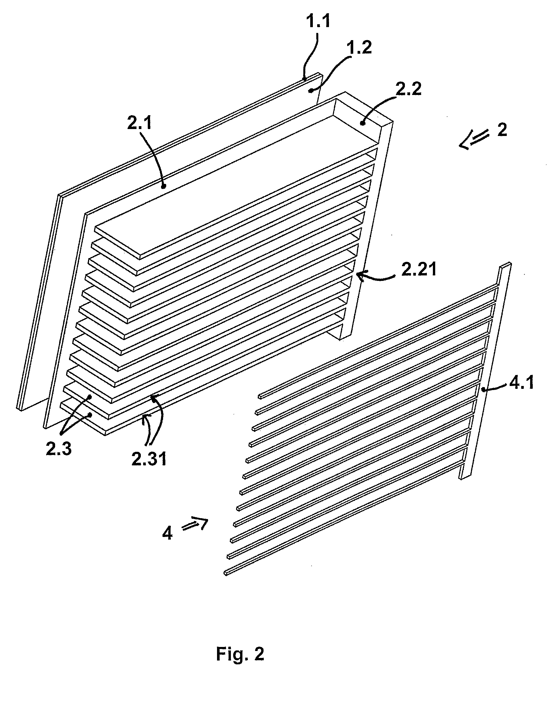
[0047]The new photovoltaic device is of the back-contacted type, i.e. it has the positive contacts (4) and the negative contacts (5) located on the rear of the device.

[0048]The new device comprises a front emitter (2) made of a p- or n-doped semiconductor material, coupled with at least one rear part (3) made of an n- or p-doped semiconductor material, the front part (2.1) of said emitter (2) being connected to a plurality of metal contacts (4) located on the rear of the device by means of one or more plates (2.3), ducts or generic elements in relief, made of a p-or n-doped semiconductor material, that pass entirely or partially through the thickness of said n- or p-doped interposed part (3).

[0049]As shown in FIG. 1, the new device has a substantially stratified design, wherein said emitter (2) comprises an extended front part (2.1), the exposed surface of which undergoes electronic passivation, preferably by means of the deposition of at least one composite layer (1.2, 1.2) typical...


PUM


Abstract

A new photovoltaic device includes at least one front emitter made of a p- or n-doped semiconductor material, coupled with at least one rear part made of an n- or p-doped semiconductor material, wherein the front part of the emitter is connected to a plurality of contacts located at the back of the device by means of one or more diffuser elements in the shape of plates, ducts or generic elements in relief made of p- or n-doped semiconductor material, which extend from the front part of the emitter through all or part of the n- or p-doped part.

Description

FIELD OF THE INVENTION[0001]The present application concerns photovoltaic devices, and more particularly concerns a new photovoltaic device of the so-called “back-contacted” type, i.e. with both the negative and the positive contacts at the back.[0002]More precisely, the present patent concerns a new photovoltaic device with an innovative architecture, the purpose of which is to maximize the device's efficiency by means of a front surface with no contacts and a structure capable of optimizing the charge collection process.SUMMARY OF THE INVENTION[0003]There are known photovoltaic devices comprising a so-called wafer, consisting of at least one p-doped semiconductor, i.e. with an excess of electronic ‘holes, coupled with at least one n-doped semiconductor, i.e. with an excess of electrons, each with their corresponding electrical contacts, wherein photon radiation on the surface of said p-doped semiconductor (adequately coated with a passivation layer) causes a charge displacement, t...

Claims


Application Information

Patent Timeline
IPC IPC(8): H01L31/00
CPCH01L31/03529Y02E10/547H01L31/0682H01L31/022458
Inventor ZARCONE, MARIANO
Owner XGROUP
Learn More