Electronic element wafer module and method for manufacturing same, electronic element module, optical element wafer module and method for manufacturing same, and electronic information device

a technology of electronic elements and wafers, applied in the direction of electric/magnetic/electromagnetic heating, instruments, television systems, etc., can solve the problems of poor positioning poor function of elements b>102/b> and signal processing circuit b>103/b>, and extremely poor manufacturing efficiency. , to achieve the effect of high positioning accuracy, high positional accuracy of internal electronic elements, and high positioning accuracy

Inactive Publication Date: 2010-06-03
SHARP KK
View PDF9 Cites 18 Cited by
  • Summary
  • Abstract
  • Description
  • Claims
  • Application Information

AI Technical Summary

Benefits of technology

[0018]The present invention is intended to solve the conventional problems described above. The objective of the present invention is to provide an electronic element wafer module, which achieves a high positional accuracy of electronic elements and a high positioning accuracy between the electronic elements and an optical aperture structure of an optical element and a light shielding film, and to achieve a high manufacturing efficiency, compared to an optical function module with the conventional module structure, and a method for manufacturing the electronic element wafer module; an optical element wafer module used for the electronic element wafer module and a method for manufacturing the optical element wafer module; an electronic element module individualized by simultaneously cutting the electronic element wafer module; and an electronic information device, such as a camera-equipped cell phone device, including the electronic element module as an image input device used in an image capturing section thereof.
[0051]Further, by precisely positioning the electronic elements and the optical elements with a high positional accuracy, precisely positioning the optical aperture structure with a certain accuracy together with the light shielding function with respect to the electronic elements and the light shielding film, and manufacturing a mask and the light shielding film at a high speed, it becomes possible to easily remove the mask and to perform the manufacturing with a simple process and at a low cost.

Problems solved by technology

As a result, if the positional accuracy of the light shielding film is poor, even the normally-functioning infrared ray light receiving element 102 and signal processing circuit 103 will start to function poorly.
This leads to an extremely poor manufacturing efficiency.
Furthermore, in the above conventional remote control light receiving module 100, the positioning of the internal elements is not accurate, and particularly, the method for manufacturing the remote control light receiving module 100 cannot be applied at all in terms of its accuracy for a camera module that requires a strict positional relationship between the light receiving portion 105 and the infrared ray light receiving element 102.

Method used


Image

  • Electronic element wafer module and method for manufacturing same, electronic element module, optical element wafer module and method for manufacturing same, and electronic information device
  • Electronic element wafer module and method for manufacturing same, electronic element module, optical element wafer module and method for manufacturing same, and electronic information device
  • Electronic element wafer module and method for manufacturing same, electronic element module, optical element wafer module and method for manufacturing same, and electronic information device

Examples


embodiment 1

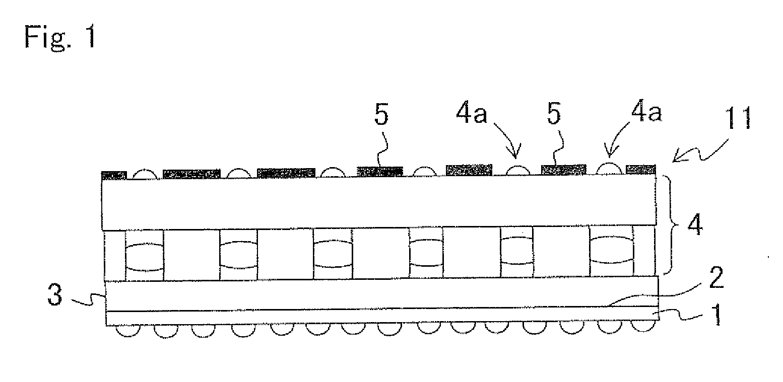
[0096]FIG. 1 is a longitudinal cross sectional view illustrating an exemplary essential part structure of a sensor wafer module according to Embodiment 1 of the present invention.

[0097]In FIG. 1, a sensor wafer module 11 according to Embodiment 1 includes: a sensor wafer 1, in which an image capturing element is provided as an electronic element on a wafer surface, the image capturing element constituted of a plurality of light receiving sections as photoelectric conversion sections (photodiodes) respectively corresponding to a plurality of pixels, and a through hole is provided between a front surface and a back surface for electrical connection; a resin adhesion layer 2 formed in the periphery of the image capturing element of the sensor wafer 1; a glass plate 3 as a cover glass for covering the image capturing element and the resin adhesion layer 2; a lens wafer module 4 provided on the glass plate 3 and including one or more lens plates laminated therein as an optical element fo...

embodiment 2

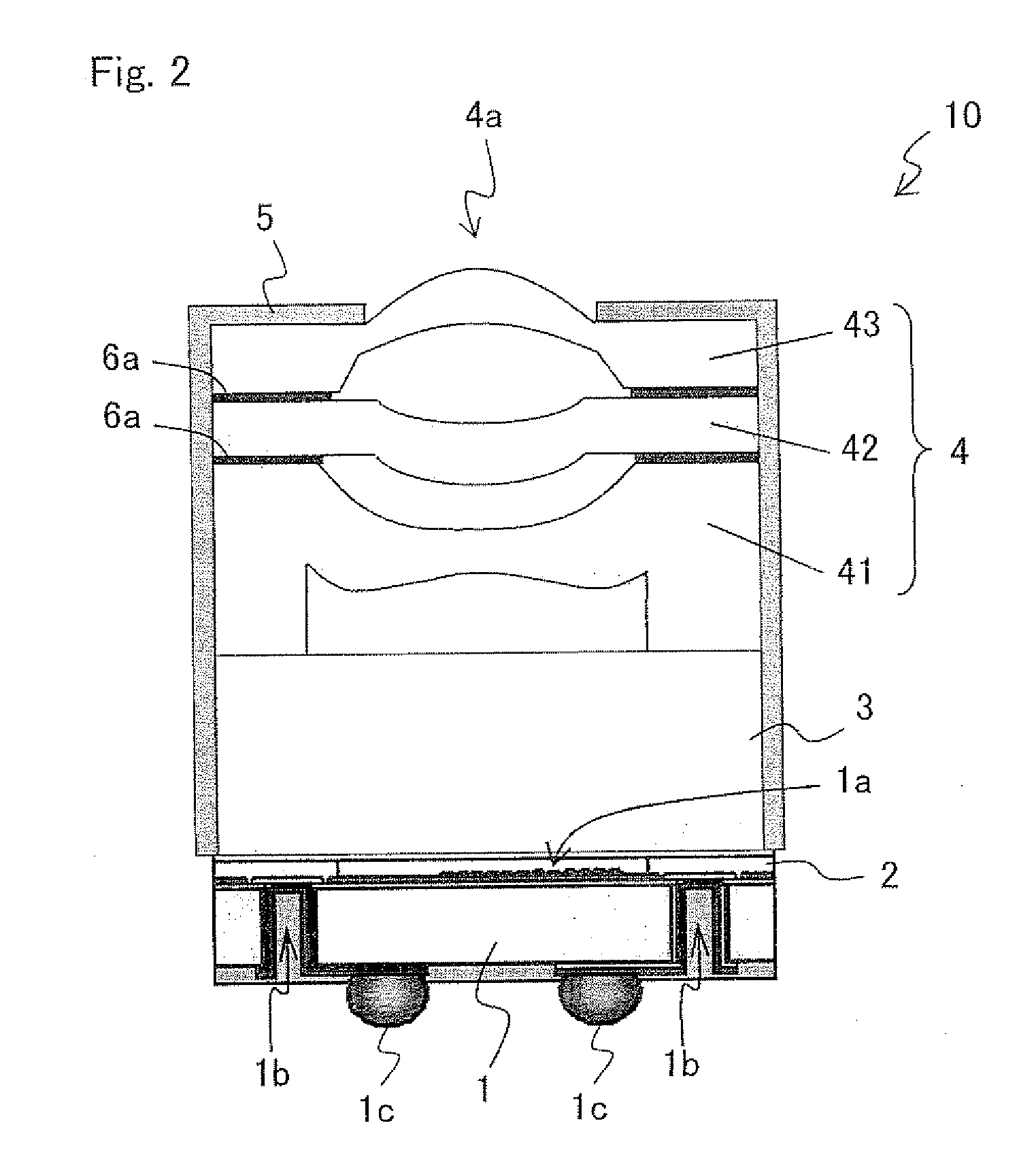
[0124]While Embodiment 1 describes the case where the lens wafer module 4 is laminated on the module TSV, and subsequently, the optical aperture is formed by the light shielding film 5 at each light opening 4a of the lens wafer module 4. Embodiment 2 describes the case where, instead of laminating the lens wafer module 4 on the module TSV, the optical aperture is formed by the light shielding film 5 at each light opening 4a of the lens wafer module 4, and subsequently, a lens wafer module 4A is laminated on the module TSV.

[0125]FIG. 7 is a longitudinal cross sectional view illustrating an exemplary essential part structure of a lens wafer module 4A according to Embodiment 2 of the present invention.

[0126]In FIG. 7, a lens wafer module 4A according to Embodiment 2 includes a lens wafer module 4, in which one or a plurality of lens plates are laminated as an optical element for focusing incident light on an image capturing element, and a light shielding film 5 formed in an area other ...

embodiment 3

[0147]While Embodiment 2 describes the case where, instead of laminating the lens wafer module 4 on the module TSV, the optical aperture is formed in the light shielding film 5 by peeling off the low-viscosity protective resin film 7 and the light shielding film 5 thereon on the light openings 4a of the lens wafer module 4, and subsequently, the lens wafer module 4A is laminated on the module TSV; Embodiment 3 describes the case where, prior to laminating the lens wafer module 4 on the module TSV, the soluble protective resin film 7A on the light openings 4a of the lens wafer module 4 is dissolved to be removed and the optical aperture is formed by the light shielding film 5, and subsequently, the lens wafer module 4 is laminated on the module TSV.

[0148]Another example of the method for manufacturing the lens wafer module 4A with the structure described above will be described in detail with reference to FIGS. 12(a) to 12(d) and FIGS. 13(a) to 13(d).

[0149]First, as illustrated in a ...


PUM

PropertyMeasurementUnit
aspect ratioaaaaaaaaaa
thicknessaaaaaaaaaa

Abstract

A method for manufacturing an electronic element wafer module is provided, the method comprising: a protective resin film forming step of forming a protective resin film on only light openings of the plurality of wafer-shaped optical elements; a light shielding film forming step of filming a light shielding film on an area except for the light openings or an entire area including the light openings; and an optical aperture forming step of removing the protective resin film, or removing the protective resin film and a light shielding film material on the protective resin film, to form an optical aperture structure by the light shielding film at the light openings.

Description

[0001]This nonprovisional application claims priority under 35 U.S.C. §119(a) to Patent Application No. 2008-306876 filed in Japan on Dec. 1, 2008, the entire contents of which are hereby incorporated by reference.BACKGROUND OF THE INVENTION[0002]1. Field of the Invention[0003]The present invention relates to an electronic element wafer module with an optical aperture structure and a method for manufacturing the electronic element wafer module; an optical element wafer module used for the electrical element wafer module and a method for manufacturing the optical element wafer module; an electronic element module individualized by simultaneously cutting the electronic element wafer module; and an electronic information device, such as a digital camera (e.g., a digital video camera or a digital still camera), an image input camera (e.g., a monitoring camera), a scanner, a facsimile machine, a television telephone apparatus and a camera-equipped cell phone device, including the electro...

Claims


Application Information

Patent Timeline
Patent Type & Authority Applications(United States)
IPC IPC(8): H01L27/00B05D5/06B32B37/12B29D11/00C23C14/28
CPCB32B2457/14H04N5/2257H01L27/14683H01L27/14618H01L2924/0002H04N23/57H01L2924/00
Inventor SUETAKE, AIJI
Owner SHARP KK
Why Eureka
Try Eureka