Semiconductor device and method for manufacturing the same
Active Publication Date: 2010-06-03
SEMICON ENERGY LAB CO LTD
View PDF101 Cites 109 Cited by
Summary
Abstract
Description
Claims
Application Information
AI Technical Summary
This helps you quickly interpret patents by identifying the three key elements:
Problems solved by technology
Method used
Benefits of technology
Benefits of technology
[0023]According to an embodiment of the present invention, in a thin film transistor in which a first oxide semiconductor region is used as an active layer, a second oxide semiconductor region having lower electrical conductivity than the first oxide semiconductor region and serving as a protective layer is formed between the first oxide semiconductor region and a protective insulating layer for the thin film transistor, whereby the second oxide semiconductor region can prevent change in composition or deterioration in film quality of the first oxide semiconductor region, and electrical characteristics of the thin film transistor can be stabilized.
[0024]By using the thin film transistor for a pixel portion and a driver circuit portion of a display device, a display device with high electrical characteristics and high reliability can be provided.
Problems solved by technology
On the other hand, although a thin film transistor using polycrystalline silicon has high field effect mobility, it takes an enormous amount of time to form the thin film transistor using polycrystalline silicon over a large-sized substrate such as a large glass substrate because a crystallization process such as laser annealing is needed.
Method used
Image
Click on the blue label to locate the original text in one second.
Reading with bidirectional positioning of images and text.
Examples
embodiment 1
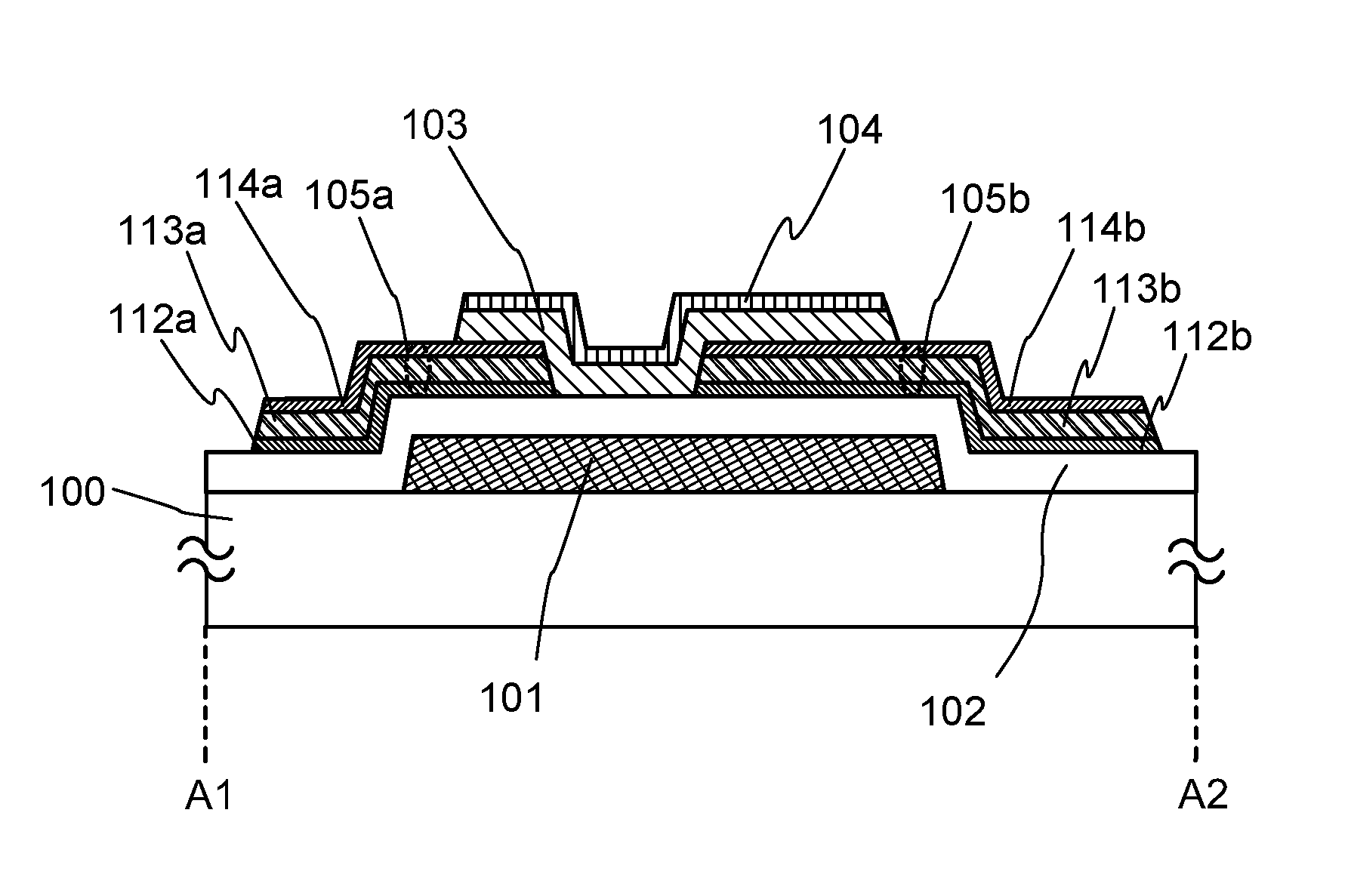
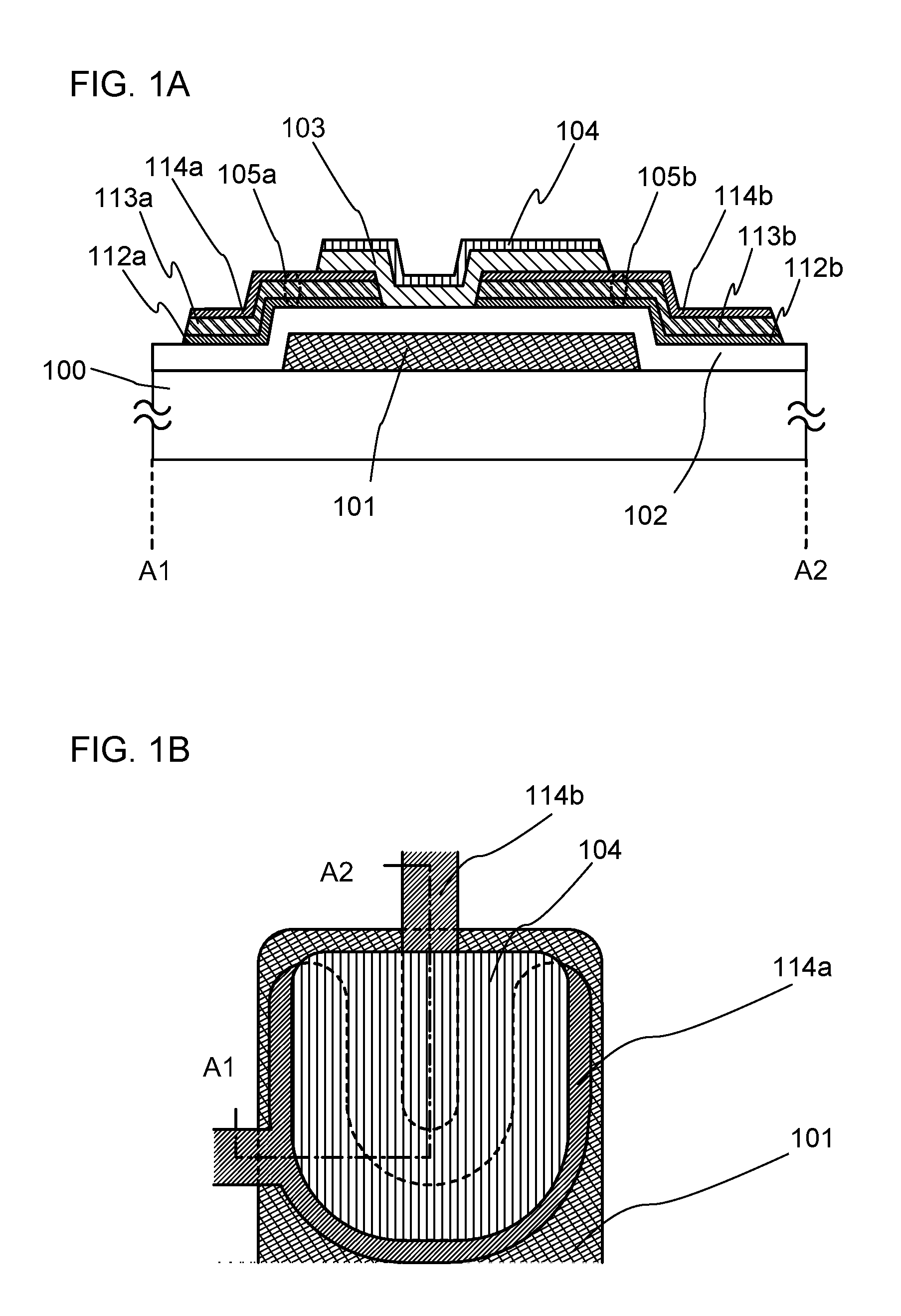
[0056]In this embodiment, a structure of a thin film transistor is described with reference to FIGS. 1A and 1B.
[0057]A thin film transistor having a bottom gate structure of this embodiment is illustrated in FIGS. 1A and 1B. FIG. 1A is a cross-sectional view, and FIG. 1B is a plan view. FIG. 1A is a cross-sectional view along line A1-A2 of FIG. 1B.
[0058]In the thin film transistor illustrated in FIGS. 1A and 1B, a gate electrode layer 101 is provided over a substrate 100, a gate insulating layer 102 is provided over the gate electrode layer 101, a source and drain electrodelayers 105a and 105b are provided over the gate insulating layer 102, a first oxide semiconductor region 103 is provided over the gate insulating layer 102 and the source and drain electrode layers 105a and 105b, and a second oxide semiconductor region 104 having lower electrical conductivity than the first oxide semiconductor region 103 is provided over the first oxide semiconductor region 103. Note that the fir...
embodiment 2
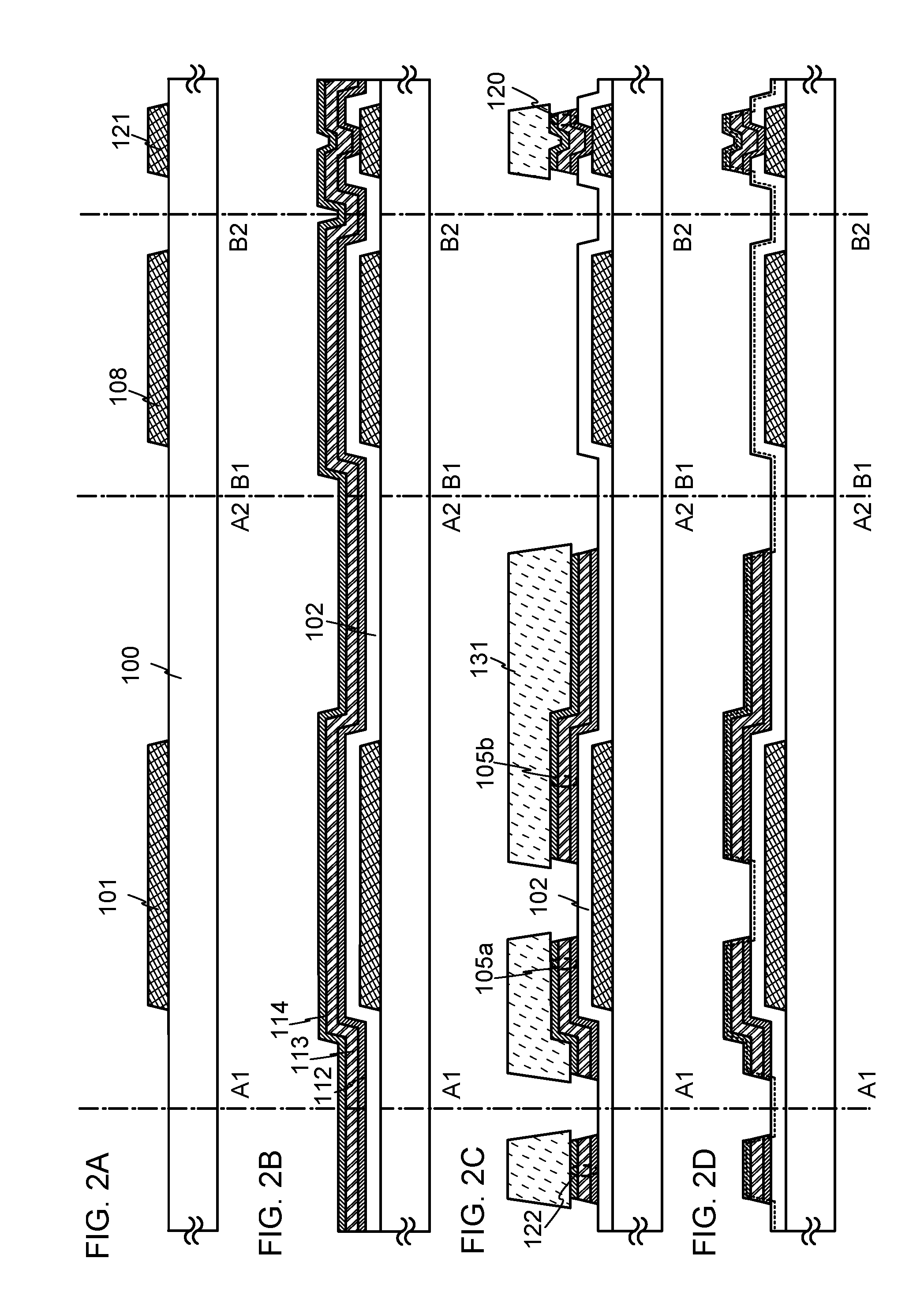
[0078]In this embodiment, a manufacturing process of a display device including the thin film transistor described in Embodiment 1 will be described with reference to FIGS. 2A to 2D, FIGS. 3A to 3C, FIG. 4, FIG. 5, FIG. 6, FIG. 7, FIGS. 8A-1, 8A-2, 8B-1, and 8B-2, and FIG. 9. FIGS. 2A to 2D and FIGS. 3A to 3C are cross-sectional views, and FIG. 4, FIG. 5, FIG. 6, and FIG. 7 are plan views. Line A1-A2 and line B1-B2 in each of FIG. 4, FIG. 5, FIG. 6, and FIG. 7 correspond to line A1-A2 and line B1-B2 in each of the cross-sectional views of FIGS. 2A to 2D and FIGS. 3A to 3C, respectively.
[0079]First, the substrate 100 is prepared. As the substrate 100, any of the following substrates can be used: non-alkaline glass substrates made of bariumborosilicate glass, aluminoborosilicate glass, aluminosilicate glass, and the like by a fusion method or a float method; ceramic substrates; plastic substrates having heat resistance enough to withstand a process temperature of this manufacturing p...
embodiment 3
[0135]In this embodiment, a thin film transistor having a different structure than that of the thin film transistor described in Embodiment 1 is described with reference to FIG. 10.
[0136]A thin film transistor having a bottom gate structure of this embodiment is illustrated in FIG. 10. In the thin film transistor illustrated in FIG. 10, the gate electrode layer 101 is provided over the substrate 100, the gate insulating layer 102 is provided over the gate electrode layer 101, the source and drain electrode layers 105a and 105b are provided over the gate insulating layer 102, buffer layers 301a and 301b are provided over the source and drain electrode layers 105a and 105b, the first oxide semiconductor region 103 is provided over the gate insulating layer 102 and the buffer layers 301a and 301b, and the second oxide semiconductor region 104 having lower electrical conductivity than the first oxide semiconductor region 103 is provided over the first oxide semiconductor region 103. Not...
Application Information
Patent Timeline
Application Date:The date an application was filed.
Publication Date:The date a patent or application was officially published.
First Publication Date:The earliest publication date of a patent with the same application number.
Issue Date:Publication date of the patent grant document.
PCT Entry Date:The Entry date of PCT National Phase.
Estimated Expiry Date:The statutory expiry date of a patent right according to the Patent Law, and it is the longest term of protection that the patent right can achieve without the termination of the patent right due to other reasons(Term extension factor has been taken into account ).
Invalid Date:Actual expiry date is based on effective date or publication date of legal transaction data of invalid patent.

