Liquid crystal display device
a liquid crystal display and display device technology, applied in non-linear optics, instruments, optics, etc., can solve problems such as image quality degradation, and achieve the effects of improving viewing angle characteristics, stable operation characteristics of thin film transistors, and improving image quality
- Summary
- Abstract
- Description
- Claims
- Application Information
AI Technical Summary
Benefits of technology
Problems solved by technology
Method used
Image

Examples
embodiment 1
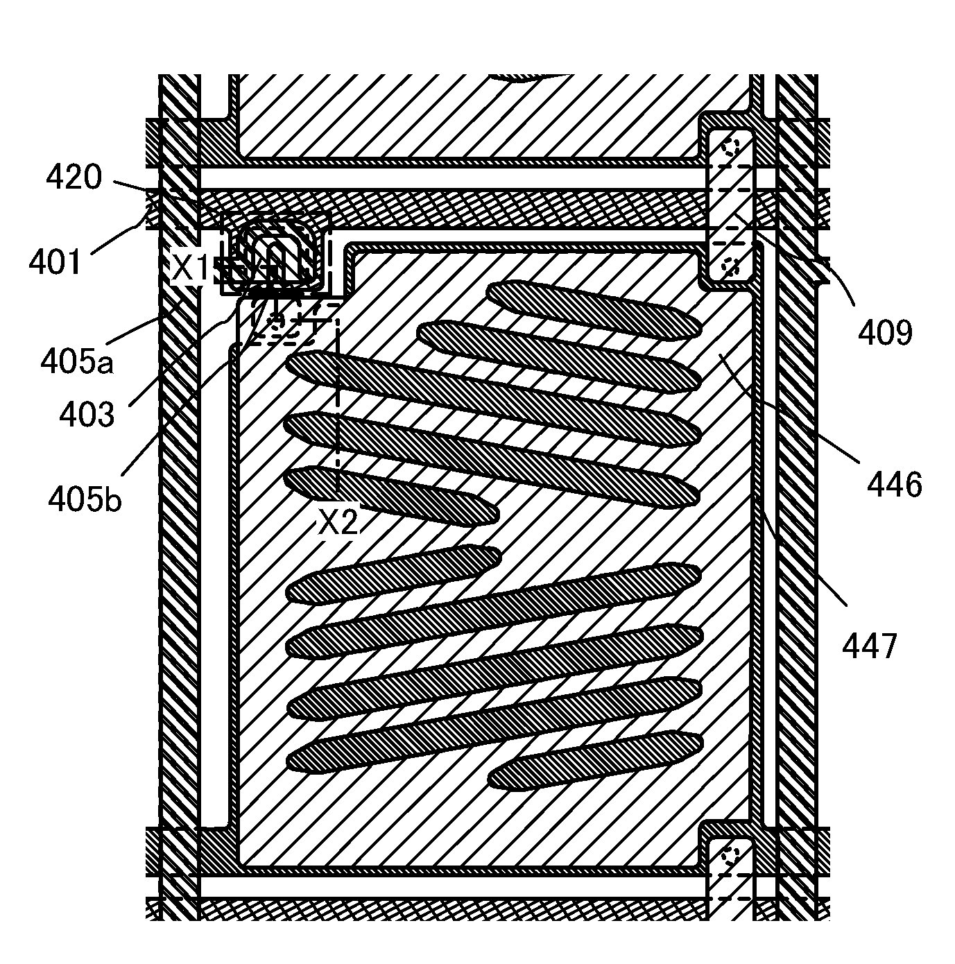
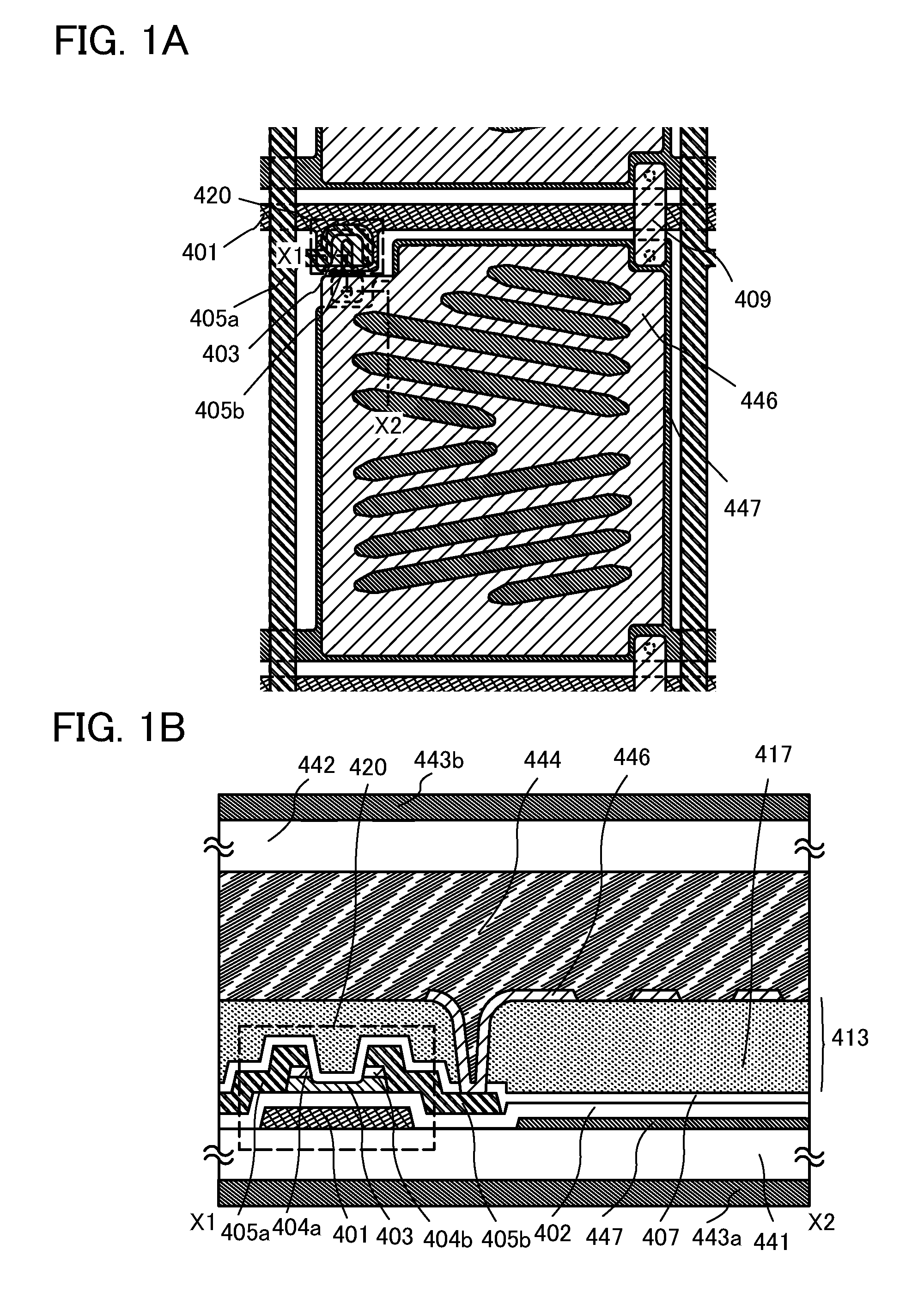
[0049]A liquid crystal display device is described with reference to FIGS. 1A and 1B.
[0050]FIG. 1A is a plan view of a liquid crystal display device and illustrates one pixel thereof. FIG. 1B is a cross-sectional view along line X1 to X2 in FIG. 1A.
[0051]In FIG. 1A, a plurality of source wiring layers (including a wiring layer 405a) are provided to be in parallel to each other (extended in a vertical direction in the drawing) and apart from each other. A plurality of gate wiring layers (including a gate electrode layer 401) are provided to be extended in a direction generally perpendicular to the source wiring layers (the horizontal direction in the drawing) and apart from each other. Common wiring layers (common electrode layers) are provided adjacent to the respective plurality of gate wiring layers and extended in a direction generally parallel to the gate wiring layers, that is, in a direction generally perpendicular to the source wiring layers (the horizontal direction in the d...
embodiment 2
[0113]Another mode of a liquid crystal display device is illustrated in FIGS. 3A and 3B. Specifically, an example of a liquid crystal display device is described, in which a first electrode layer in a flat-plate shape formed in a lower layer is used as a pixel electrode layer, and a second electrode layer having an opening pattern formed in an upper layer is used as a common electrode layer. Note that components in common with those in Embodiment 1 can be formed using the similar material and the similar manufacturing method, and detailed description of the same portions and portions which have similar functions is omitted.
[0114]FIG. 3A is a plan view of a liquid crystal display device and illustrates one pixel thereof. FIG. 3B is a cross-sectional view along line X1 to X2 in FIG. 3A.
[0115]In FIG. 3A, a plurality of source wiring layers (including the wiring layer 405a) are provided in parallel to each other (extended in a vertical direction in the drawing) and apart from each other...
embodiment 3
[0120]Other modes of liquid crystal display devices are illustrated in FIGS. 4A and 4B and FIGS. 7A and 7B. Specifically, structural examples are described, in each of which a first electrode layer is provided above a thin film transistor. Note that components in common with those in Embodiments 1 and 2 can be formed using the similar material and the similar manufacturing method, and detailed description of the same portions and portions which have similar functions is omitted.
[0121]FIG. 4A and FIG. 7A are each a plan view of a liquid crystal display device and each illustrate one pixel. FIG. 4B and FIG. 7B are cross-sectional views of FIG. 4A and FIG. 7A along line X1 to X2, respectively.
[0122]In each plan view of FIG. 4A and FIG. 7A, in a manner similar to Embodiment 2, a plurality of source wiring layers (including the wiring layer 405a) are provided in parallel to each other (extended in a vertical direction in the drawing) and apart from each other. A plurality of gate wiring ...
PUM
| Property | Measurement | Unit |
|---|---|---|
| temperature | aaaaa | aaaaa |
| transmittance | aaaaa | aaaaa |
| sheet resistance | aaaaa | aaaaa |
Abstract
Description
Claims
Application Information
 - Generate Ideas
- Intellectual Property
- Life Sciences
- Materials
- Tech Scout
- Unparalleled Data Quality
- Higher Quality Content
- 60% Fewer Hallucinations
Browse by: Latest US Patents, China's latest patents, Technical Efficacy Thesaurus, Application Domain, Technology Topic, Popular Technical Reports.
© 2025 PatSnap. All rights reserved.Legal|Privacy policy|Modern Slavery Act Transparency Statement|Sitemap|About US| Contact US: help@patsnap.com