Semiconductor device and method for manufacturing the same

a semiconductor and semiconductor technology, applied in the direction of microstructural devices, microstructured devices, instruments, etc., can solve the problems of reducing the manufacturing yield of the sensor, complicated manufacturing process, damage to the connection and conduction of the device, etc., and achieve the effect of improving the bonding strength between the first chip and the second chip and improving the productivity of the semiconductor devi

Active Publication Date: 2010-06-17
DENSO CORP
View PDF10 Cites 69 Cited by
  • Summary
  • Abstract
  • Description
  • Claims
  • Application Information

AI Technical Summary

Benefits of technology

[0025]In the above method, the first concavity of the second wiring layer in the first chip is not covered with the fourth wiring layer of the second chip. Further, the second concavity of the fourth wiring layer in the second chip is not covered with the second wiring layer in the first chip. Thus, a bonding a

Problems solved by technology

Thus, connection and conduction in the device may be damaged.
However, in the techniques disclosed in JP-A-H09-129898, JP-A-H11-295336, and JP-A-H06-123628, since the wiring layer made of poly crystal silicon is formed on the

Method used


Image

  • Semiconductor device and method for manufacturing the same
  • Semiconductor device and method for manufacturing the same
  • Semiconductor device and method for manufacturing the same

Examples


second embodiment

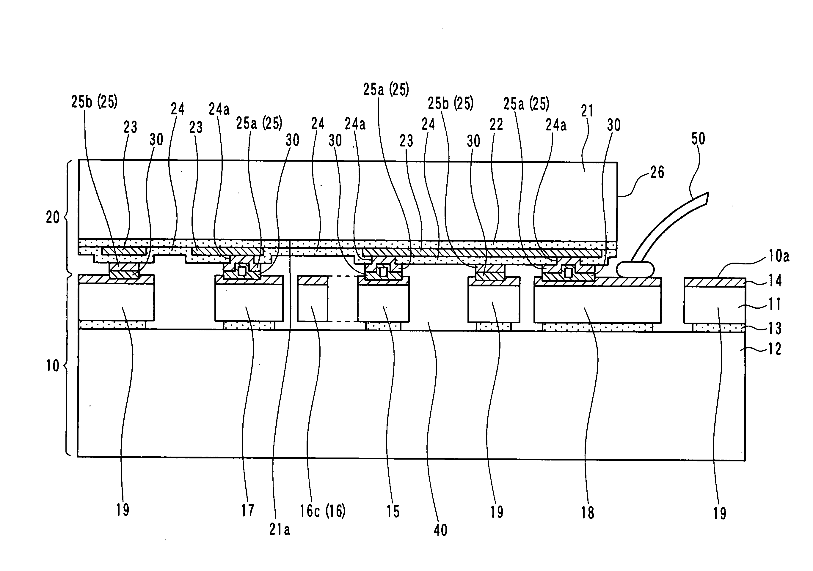
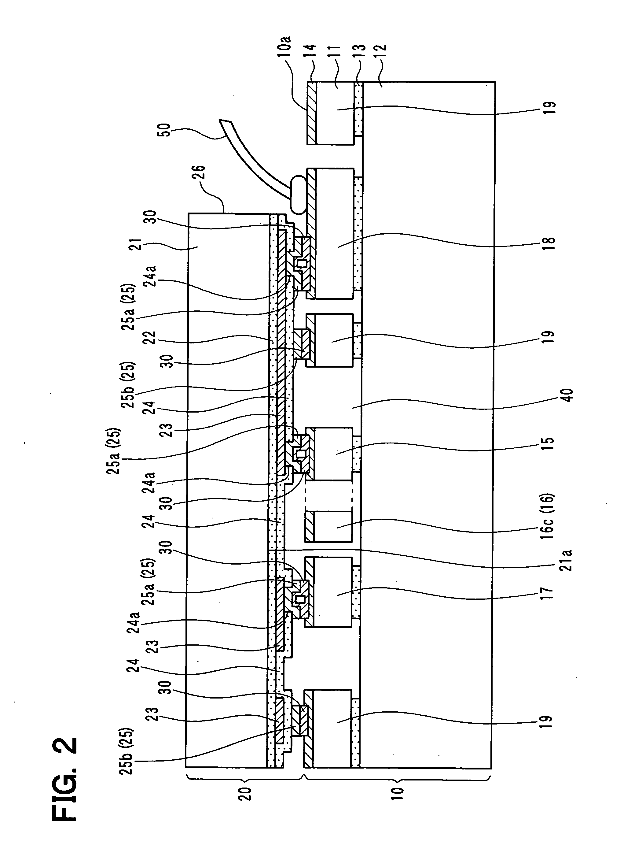
[0128]In the first embodiment, the wiring layer 14 in the sensor portion 10 covers the concavities on the wiring portion 25a, and then, the eutectic alloy between the wiring layer 14 and the wiring portion 25a is formed. In the second embodiment, the wiring layer 14 is bonded to the flat surface of the wiring portion 25a.

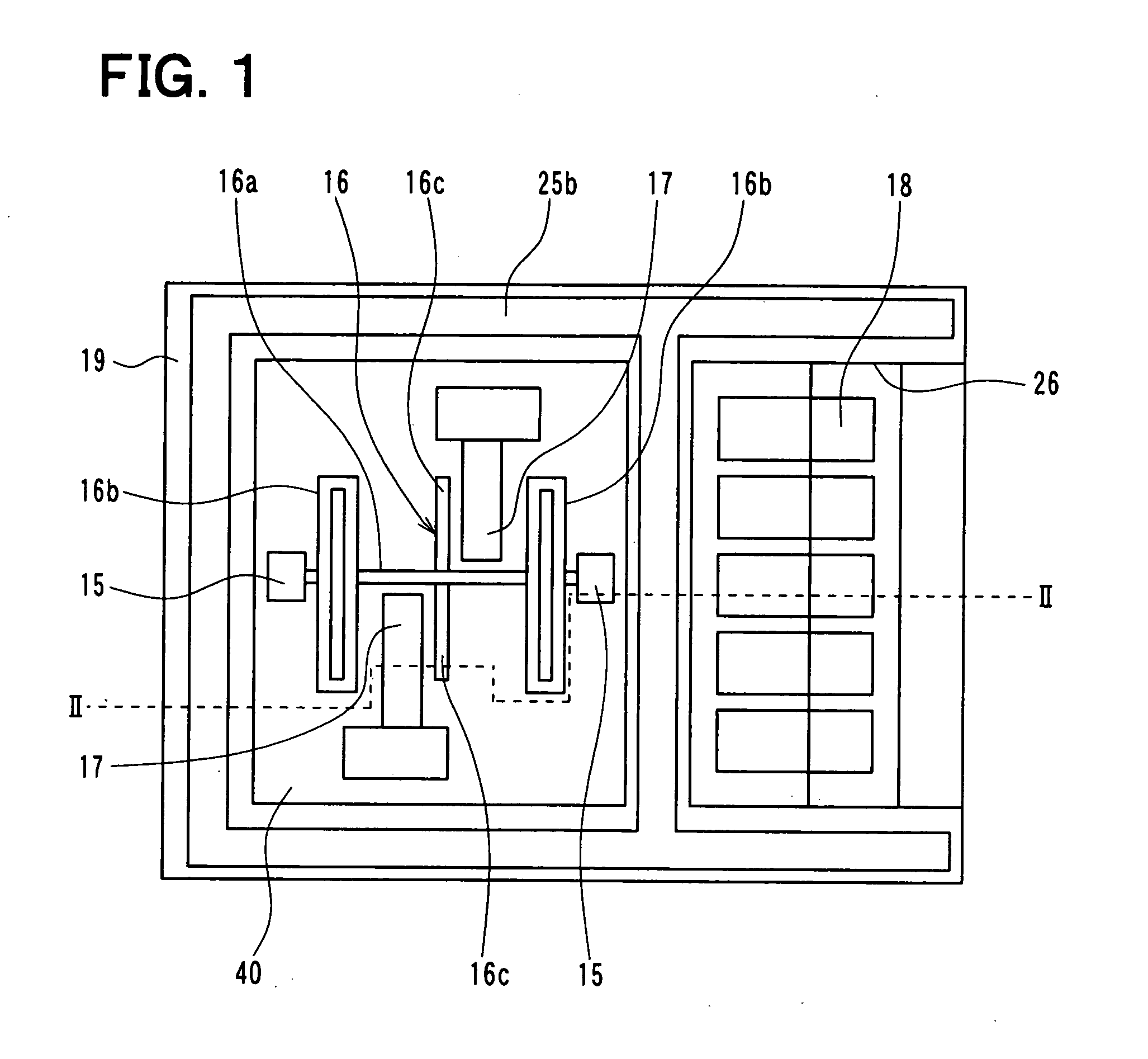
[0129]FIG. 8 shows a bonding state of the sensor portion 10 and the cap portion 20. FIG. 8 corresponds to FIG. 6.

[0130]In FIG. 8, a part of the wiring portion 25a of the second wiring layer 25, which is embedded in the opening 24a of the second insulation film 24, is concaved because of a step coverage effect, so that the surface of the wiring portion 25a has a concavity. This concavity has a bottom, and is formed in such a manner that the surface of the wiring portion 25a of the second wiring layer 25 is concaved toward the first wiring layer 23.

[0131]Since the conductive layer 60 is formed on the surface of the wiring portion 25a, the conductive layer 60 has a su...

third embodiment

[0137]In the first and second embodiments, the concavity of wiring portion 25a is formed on the opening 24a in the second insulation film 24 because of the step coverage. In the third embodiment, the concavity is not formed on the wiring portion 25a.

[0138]In the step of forming the cap portion 20, the opening 24a is formed ion the second insulation film 24 in the steps in FIGS. 5A to 5C.

[0139]Then, in a step of FIG. 9A, the aluminum layer as the second wiring layer 25 is formed on the second insulation film 24 and the first wiring layer 23 exposed in the opening 24a of the second insulation film 24. Then, the second wiring layer 25 is flattened by a CMP polishing method. Thus, the concavity of the wiring portion 25a is removed. The surface of the second wiring layer 25 is flat without concavity. After that, the conductive layer 60 is formed on the flat surface of the second wiring layer 25.

[0140]As shown in FIG. 9B, the second wiring layer 25 and the conductive layer 60 are pattern...

fourth embodiment

[0142]In the first embodiment, the second wiring layer 25 is made of aluminum. In this embodiment, the second wiring layer 25 is replaced with eth conductive layer 60.

[0143]FIG. 10 shows a semiconductor device according to a fourth embodiment. The conductive layer 60 is formed on the second insulation film 24 and the first wiring layer 23 exposed in the opening 24a of the second insulation film 24. Further, the conductive layer 60 is patterned so as to form the wiring portion 25a and the sealing portion 25b. The conductive layer 60 is made of germanium.

[0144]A part of the wiring layer 14 and a part of the conductive layer 60 are alloyed to be eutectic alloy, and the eutectic alloy portion 30 is formed. Specifically, the wiring portion 25a and the sealing portion 25b are bonded to the sensor portion 10 via the eutectic alloy portion 30. In this case, the device does not include the second wiring layer 25, compared with the device shown in FIG. 6. Accordingly, in the device, one alumi...


PUM


Abstract

A semiconductor device includes: a sensor including a sensor structure on a first side of the sensor and a periphery element surrounding the sensor structure; and a cap covering the sensor structure and having a second side bonded to the first side of the sensor. The cap includes a first wiring layer on the second side of the cap. The first wiring layer steps over the periphery element. The sensor further includes a sensor side connection portion, and the cap further includes a cap side connection portion. The sensor side connection portion is bonded to the cap side connection portion. At least one of the sensor side connection portion and the cap side connection portion provides an eutectic alloy so that the sensor side connection portion and the cap side connection portion are bonded to each other.

Description

CROSS REFERENCE TO RELATED APPLICATIONS[0001]This application is based on Japanese Patent Applications No. 2008-321218 filed on Dec. 17, 2008, No. 2008-330252 filed on Dec. 25, 2008, and No. 2009-138031 filed on Jun. 9, 2009, the disclosures of which are incorporated herein by reference.FIELD OF THE INVENTION[0002]The present invention relates to a semiconductor device and a method for manufacturing a semiconductor device.BACKGROUND OF THE INVENTION[0003]Conventionally, an inertia force sensor having a device layer, an upper substrate and a lower substrate is proposed in, for example, JP-A-2004-333133. The device layer includes a movable portion and the like. The upper substrate is bonded to the upper side of the device layer, and the lower substrate is bonded to the lower side of the device layer. Thus, the movable, portion in the device layer is sealed with the upper and lower substrates. The upper substrate functions as a cap layer for covering the movable portion so that the upp...

Claims


Application Information

Patent Timeline
IPC IPC(8): H01L25/065H01L23/48H01L23/522H01L21/60H01L21/768H01L21/822
CPCB81B7/007B81B2207/097H01L2924/1461H01L2224/80001G01P2015/0814G01C19/5719G01P15/0802G01P15/125H01L23/481H01L24/11H01L24/12H01L24/16H01L24/48H01L24/73H01L24/94H01L25/0657H01L25/16H01L2224/05558H01L2224/114H01L2224/116H01L2224/13009H01L2224/13025H01L2224/13099H01L2224/13144H01L2224/2518H01L2225/06513H01L2225/06541H01L2924/01002H01L2924/01013H01L2924/01015H01L2924/01018H01L2924/01022H01L2924/01029H01L2924/01032H01L2924/01047H01L2924/01079H01L2924/01322H01L2924/10157H01L2924/10329H01L2924/14H01L2924/19041H01L2924/30105H01L2924/3025H01L2224/13011H01L2924/01006H01L2924/01033H01L2924/01072H01L2924/014H01L2224/48H01L2924/10253H01L2224/0401H01L2924/00H01L2924/15747H01L2924/15787H01L2924/15788H01L2224/81805H01L2224/48463G01C19/5783H01L2924/00014H01L2224/45144H01L24/45H01L2224/023H01L2224/45015H01L2924/207H01L2924/0001
Inventor FUJI, TETSUOYAMANAKA, AKITOSHIYOKURA, HISANORI
Owner DENSO CORP
Why Eureka
Try Eureka