

Solid electrolytic capacitor and method for manufacturing the same
a technology of electrolyte capacitors and solid electrolyte, which is applied in the direction of electrolytic capacitors, liquid electrolytic capacitors, transportation and packaging, etc., can solve the problem of difficulty in reducing the esr to the desired low level
- Summary
- Abstract
- Description
- Claims
- Application Information
AI Technical Summary
Benefits of technology
Problems solved by technology
Method used
Image

Examples
examples
[0105]The invention will now be specifically described by the following typical examples that are mere illustration and by no means limit the scope of the invention.
examples 1-4
, Comparative Examples 1-8
[0106]Approximately 0.1 g of a niobium powder was put in a hopper of a tantalum element automatic molding machine (“TAP-2R” available from SEIKEN Co., Ltd.) where the niobium powder was automatically molded together with a niobium wire with a 0.3 mm diameter into a molding having a size of 4.5 mm×3.0 mm×1.8 mm. The molding was left to stand at a temperature of 1,250° C. under a reduced pressure of 4×10⁻³ Pa for 30 minutes to give a sintered body.
[0107]30 pieces of the sintered bodies were subjected to electrochemical formation in an aqueous 0.1% phosphoric acid solution at a voltage of 20V for 200 minutes to form a dielectric oxide film on the surface of each sintered body. Then the sintered bodies were contacted with an equi-volume mixed liquid of an aqueous 10% ammonium persulfate solution and an aqueous 0.5% anthraquinonesulfonic acid and then exposed to a pyrrole vapor. This procedure of contacting with the mixed liquid and then exposing to a pyrrole va...
examples 5-8
, Comparative Examples 9-16
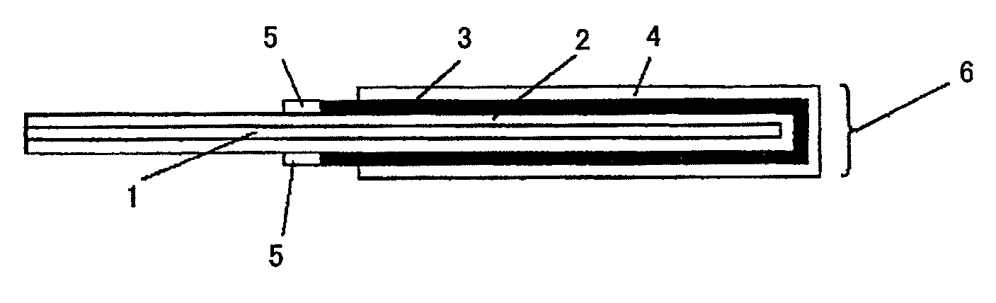
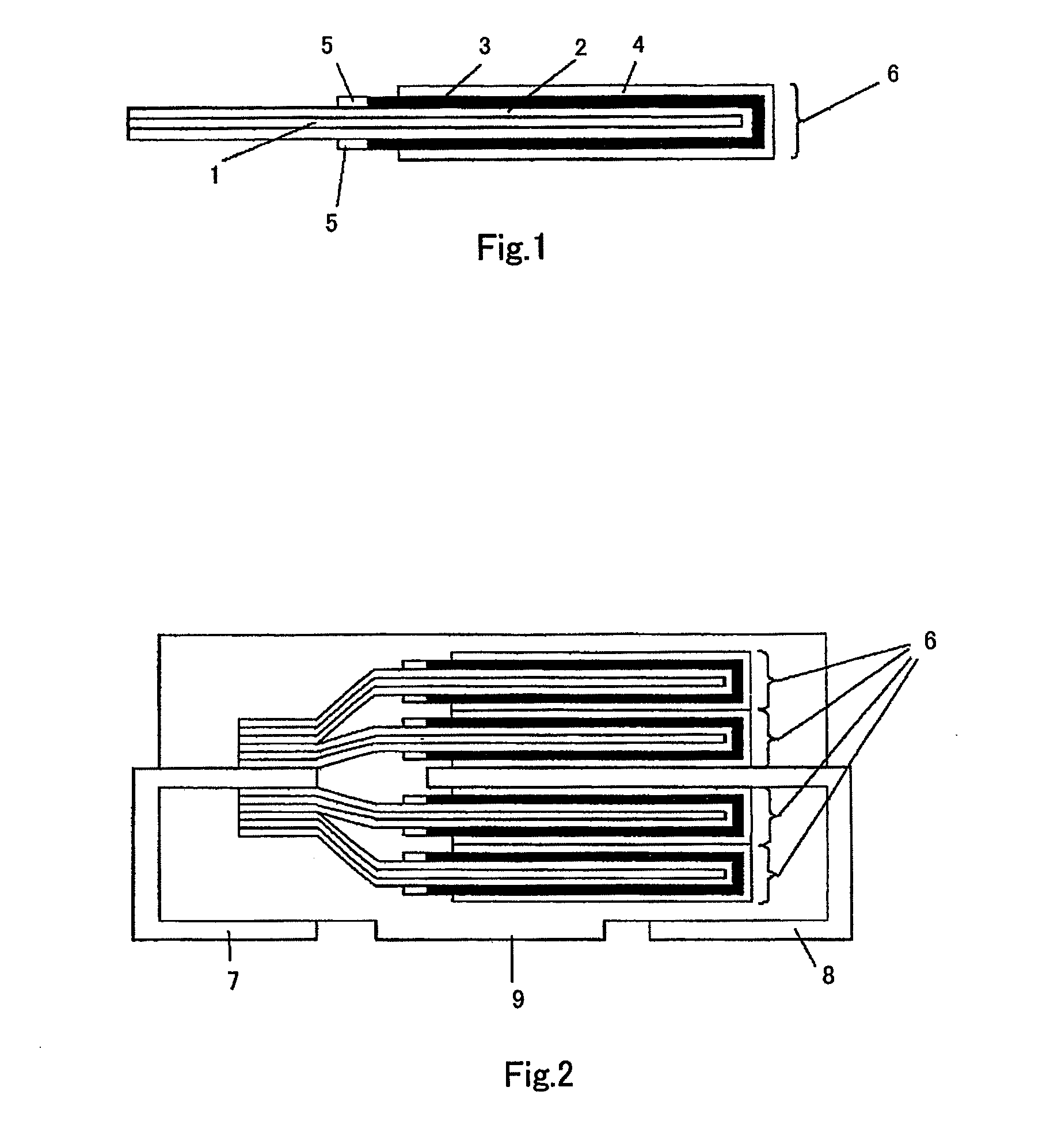
[0112]A single sheet solid electrolyte capacitor element having a structure shown in FIG. 1 was made as follows.
[0113]An etched aluminum foil [anode substrate (1)] having an alumina dielectric film formed on the surface thereof was cut into a desired size (thickness 80 μm, length 7 mm and width 3 mm). One end portion thereof having a length of 1 mm and a width of 3 mm was an anode portion. An insulating film with a width of 1 mm was wound around in a region adjacent to the anode portion of the aluminum foil, to form an insulating layer (5). The portion having a length of 4 mm and a width of 3 mm, which is other than the anode portion and the insulating layer-formed portion, was subjected to chemical formation by treating with an aqueous ammonium adipate solution having a concentration of 10% by mass at 20 V to form a dielectric film (2) on the end portion including the cut surface. The substrate was then immersed in an aqueous solution containing 15% by ma...
PUM
| Property | Measurement | Unit |
|---|---|---|
| particle diameter | aaaaa | aaaaa |
| particle diameter | aaaaa | aaaaa |
| particle diameter | aaaaa | aaaaa |
Abstract
Description
Claims
Application Information