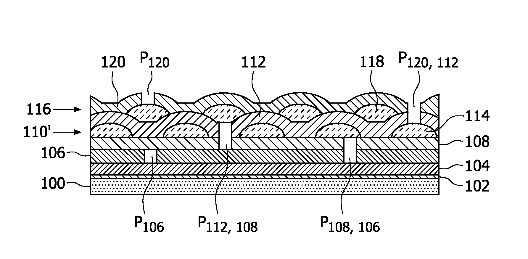
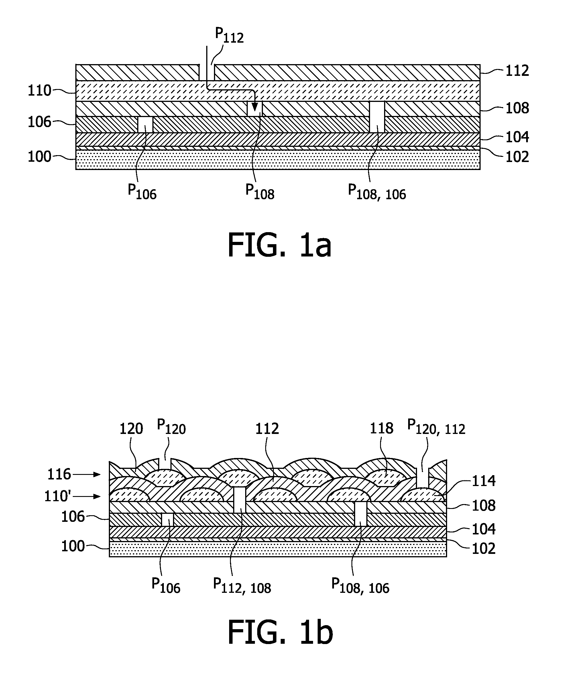
[0008]According to an aspect of the invention, the above object is met by an encapsulation for an electronic thin film device, comprising a first barrier layer, a second barrier layer, and a first planarization layer for reducing the formation of pinholes in a subsequent barrier layer, said first planarization layer arranged between the first barrier layer and the second barrier layer, wherein the first planarization layer is composed of a first plurality of planarization segment having areas formed between each other, and the encapsulation further comprises a second planarization layer arranged between the second barrier layer and a third barrier layer, wherein the second planarization layer is composed of a second plurality of planarization segments arranged to extend over the areas between the first plurality of planarization segments, thereby further reducing the number of pinholes providing passageways through the encapsulation.
[0010]However, according to the invention, by arranging the barrier layers and the planarization layers in a horizontal multi-layer encapsulation stack, where planarization segments in each of the layers are essentially decoupled from each other and in practice non-interconnecting with each other, it is possible to limit the lateral transportation of water and oxygen through the planarization layer. Instead, if water / oxygen enters the top barrier layer, and eventually a planarization segment, it is contained in the “sphere” of a planarization segment, having a minimized possibility of entering a pinhole in a subsequent barrier layer. Other advantages that follows using direct thin-film encapsulation includes, as mentioned above, thinner and / or lighter and / or mechanically more flexible packages.
[0015]In an embodiment of the present invention, the active area comprises a light-emitting layer, an
anode and a cathode, thereby forming a light-emitting
diode (LED). Such an LED can for example be a
small molecule light-emitting device (
OLED) or a polymeric light-emitting
diode (PLED), or similar. As mentioned earlier, the proper encapsulation of an
OLED device is extremely important for reaching a high manufacturing yield and long lifetime of the device. In a
OLED / PLED device, if water / oxygen is to come in contact with the cathode (through particle induced pinholes in the device), the interaction will result in inactive parts (black spots) in the OLED / PLED. These spots are perfect spheres, and the area grows linearly in time.
[0016]Therefore, by using an encapsulation according to the present invention for the encapsulation of a light-emitting
diode, the absence of water / oxygen in the pinholes in the cathode, which are on the sub-
micron scale, will therefore not result in the formation of defects that are visible by the
naked eye. Furthermore, the presence of pinholes will not result in a reduction of the intrinsic lifetime of the light-emitting device by an early failure that corresponds to the rejection of a device on basis of the occurrence of a
black spot.
[0017]Preferably, at least one of the barrier layers is formed by a
Silicon Nitride (SiN) layer. One single barrier layer formed using
Silicon Nitride generally covers 90-99% of the particles / pinholes, and the oxygen /
water barrier properties of SiN is good enough to prevent water / oxygen to penetrate through the SiN barrier layer for many 10,000's of hours. However, the remaining 1-10% uncovered pinholes are the problem, and therefore, use of the decoupled planarization segments according to the present invention provides a promising solution to the prior art water / oxygen problematic pinhole induced pathways to the active area of the electronic device. Other barrier materials are also contemplated, however, to provide adequate barrier properties, the water
penetration rate for a barrier layer should preferably be at approximately one
microgram / m2 / day. However, the water
penetration rate can range from 5 to 0.1
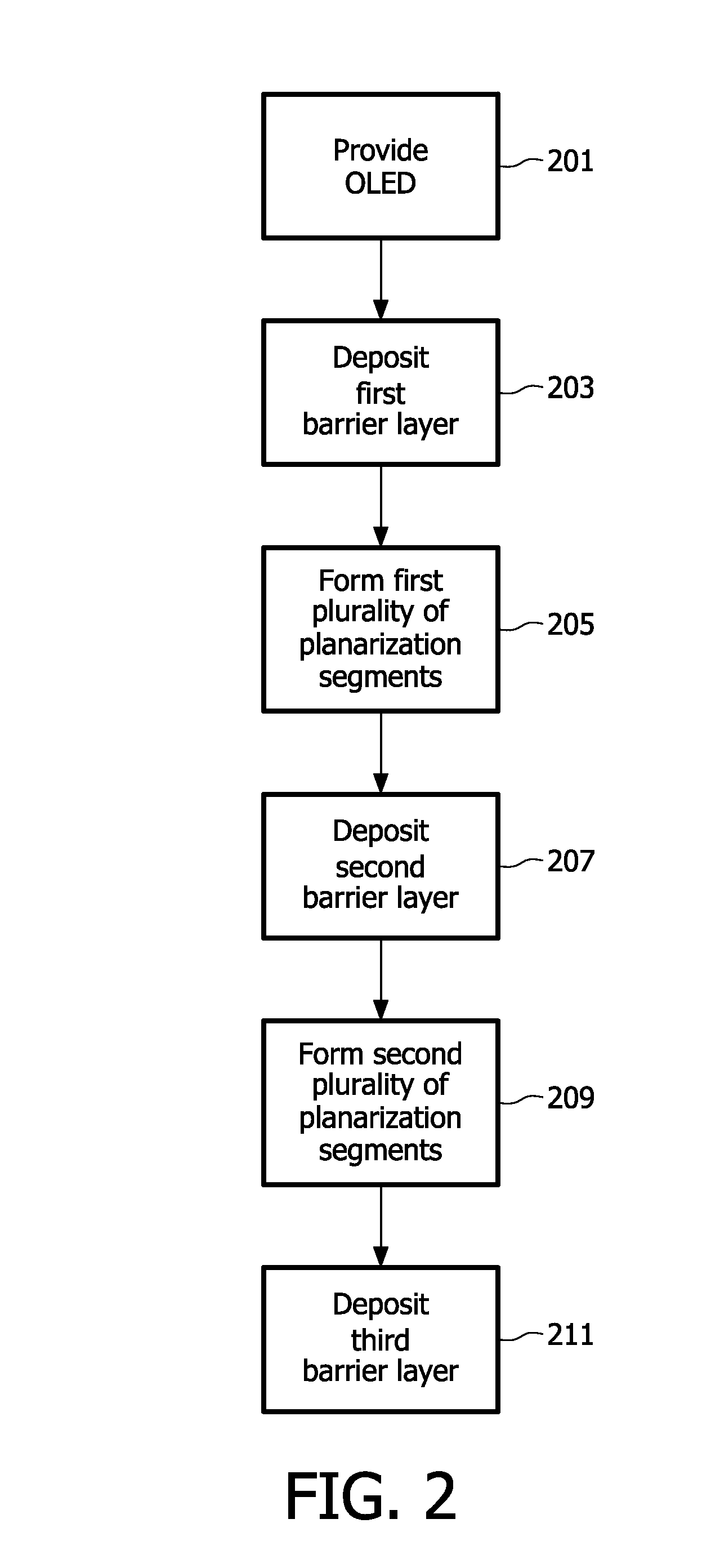
microgram / m2 / day. According to a further aspect of the invention, there is provided a method for the formation of an encapsulation for an electronic thin film device, comprising the steps of forming a first barrier layer, arranging a first planarization layer on top of the first barrier layer, the first planarization layer provided for reducing the formation of pinholes in a subsequent barrier layer, and forming a second barrier layer on top of the first planarization layer, wherein the first planarization layer is composed of a first plurality of planarization segment having areas formed between each other, wherein the method further comprises the steps of arranging a second planarization layer on top of the second barrier layer, and forming a third barrier layer on top of the second planarization layer, wherein the second planarization layer is composed of a second plurality of planarization segments arranged to extend over the areas between the first plurality of planarization segments, thereby further reducing the number of pinholes providing passageways through the encapsulation.
[0018]This aspect of the invention provides similar advantages as according to the above discussed encapsulation for an electronic thin film device, including increased lifetime at the same time as the number of defects in the form of pinhole induced inactive parts in the electronic thin film device are reduced.
