Method for detecting a weak point

a weak point and detection method technology, applied in the field of detecting a weak point, can solve the problems of affecting adjacent patterns, distorted patterns, and distortion of patterns projected onto semiconductor substrates through exposure processes, and achieve the effect of optical proximity effect compensation of target layou

Inactive Publication Date: 2010-06-24
SK HYNIX INC
View PDF12 Cites 10 Cited by
  • Summary
  • Abstract
  • Description
  • Claims
  • Application Information

AI Technical Summary

Benefits of technology

[0014]According to an embodiment of the present invention, a method for detecting a weak point comprises: providing a target layout; compensating for an optical proximity effect on the target layout; and determining whether or not the optical proximity effect compensation of the...

Problems solved by technology

As the pattern gradually becomes minute due to a high integration of the semiconductor device, the patterns which are projected onto the semiconductor substrate through an exposure process can become distorted from the real image of an exposure mask pattern.
Particularly, if a gap between adjacent patterns is short among exposure mask patterns, ...

Method used


Image

  • Method for detecting a weak point
  • Method for detecting a weak point
  • Method for detecting a weak point

Examples


Embodiment Construction

[0029]Hereinafter, an embodiment of the present invention will be illustrated with reference to the attached drawings.

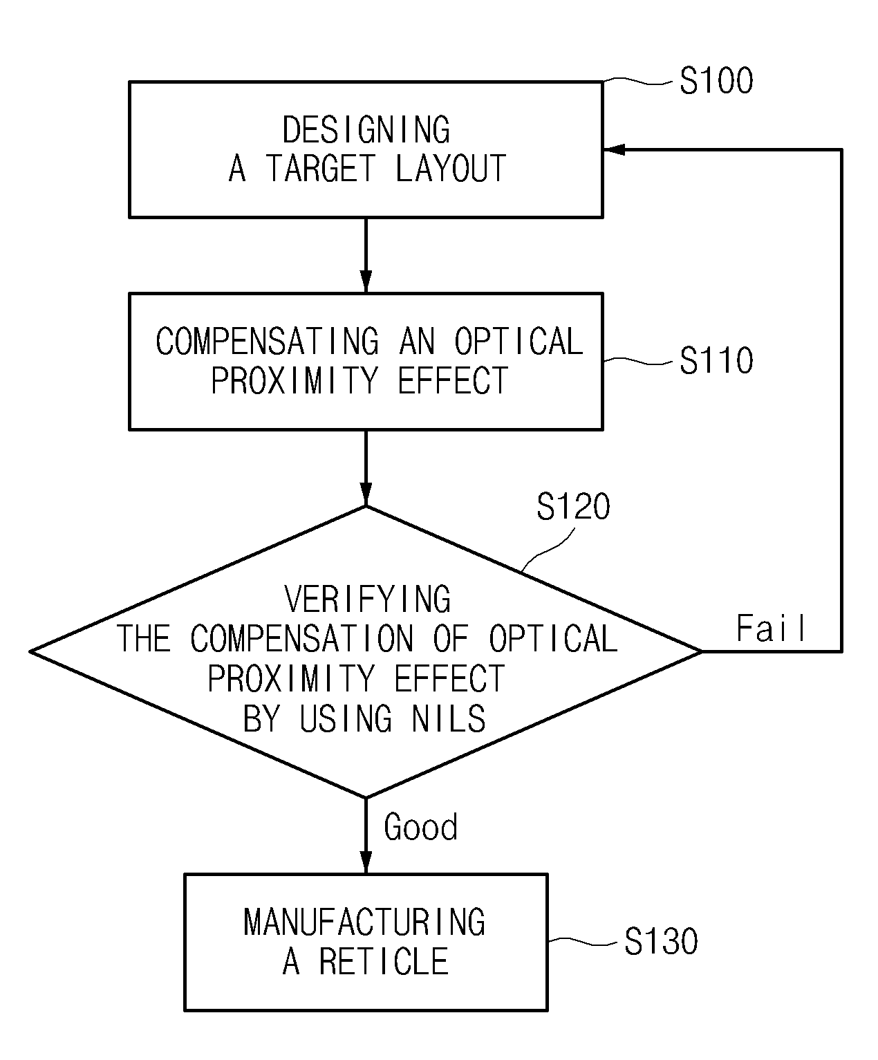
[0030]FIG. 2 is a flowchart which makes a final exposure mask by using a method for detecting a mask error enhancing factor of the present invention.

[0031]A target layout is designed (S100). Here, the target layout can be a layout including a new design capable of improving a design for the characteristic enhancement of a semiconductor device or a process margin.

[0032]Then, an optical proximity effect compensation for the target layout, e.g., an optical proximity correction, is performed (S110). This predicts the image of a final pattern by simulation modeling, and then performing a calibration through the pattern implemented as a distorted form.

[0033]The calibration can be understood as a process of minimizing the difference between the target layout and the distorted pattern by using a method of adding or removing patterns which are lower than an exposure mask reso...


PUM


Abstract

A weak point detecting method of the present invention designs a target layout, and compensates an optical proximity effect for the target layout, thereafter, verifies the target layout in which the optical proximity effect is compensated by using an NILS of the target layout, thereby, enabling to reduce the time and cost in detecting a weak point for a full chip regardless of the size and form of a pattern.

Description

CROSS-REFERENCE TO RELATED APPLICATION[0001]The priority of Korean patent application No. 10-2008-0130113 filed on Dec. 19, 2008, the disclosure of which is hereby incorporated in its entirety by reference, is claimed.BACKGROUND OF THE INVENTION[0002]The present invention relates to a method of detecting a weak point in an exposure mask, and more particularly, to a method of detecting a weak point using a NILS (Normalized Image Log Slope).[0003]Generally, an exposure mask (reticle) is required in addition to an exposure apparatus and a photoresist to form a pattern used for a photolithography process to produce a semiconductor. The exposure mask is an original plate which is used to repetitively form a pattern on a semiconductor substrate. It is made of a formed quartz plate of a chrome pattern having four or five times the size of the target pattern according to the reduction projection rate. The pattern on this exposure mask should have the same critical dimension for the same lay...

Claims


Application Information

Patent Timeline
IPC IPC(8): G06F17/50
CPCG03F1/36G06F17/5081G06F2217/12Y02P90/265G03F1/84G06F30/398G06F2119/18Y02P90/02G03F7/70441G03F1/68
Inventor KIM, CHEOL KYUN
Owner SK HYNIX INC
Why Eureka
Try Eureka