Light emitting device having plurality of non-polar light emitting cells and method of fabricating the same

a light emitting cell and non-polar technology, applied in the direction of semiconductor/solid-state device manufacturing, semiconductor devices, electrical devices, etc., can solve the problems of difficult to increase the thickness of a light emitting layer, reduce the luminous power of the light emitting layer, and cost a great deal to grow a nitride semiconductor. , to achieve the effect of excellent crystallinity and saving fabrication costs

Active Publication Date: 2010-07-01
SEOUL VIOSYS CO LTD
View PDF18 Cites 78 Cited by
  • Summary
  • Abstract
  • Description
  • Claims
  • Application Information

AI Technical Summary

Benefits of technology

[0017]Exemplary embodiments of the present invention also provide a light emitting device having a plurality of non-polar light emitting cells, which can have excellent crystallinity and save fabrication costs, and a method of fabricating the same.
[0018]Exemplary embodiments of the present invention also provide a light emitting device having a plurality of light emitting cells, in which a short circuit in a light emitting cell due to metallic etch byproducts can be prevented, and a method of fabricating the same.
[0019]Exemplary embodiments of the present invention also provide a light emitting device, in which a reflective metal layer can be prevented from being deteriorated due to etching or oxidation, and a method of fabricating the same.

Problems solved by technology

Therefore, it is difficult to increase the thickness of a light emitting layer, and there is a limitation in improving luminous power due to a decrease in light emitting recombination rate.
However, it costs a great deal to grow a nitride semiconductor using a GaN substrate grown on a sapphire substrate.
Further, it is not easy to obtain a nitride semiconductor that has crystallinity superior to that of a c-plane nitride semiconductor.
Meanwhile, LEDs generally emit light by forward current and require supply of DC current.
However, since the light emitting device has light emitting elements (hereinafter, light emitting cells) formed on a substrate used as a growth substrate, e.g., a sapphire substrate, the light emitting cells have a limitation in structure, and there is a limitation in improving light extraction efficiency.
However, in the prior art, while the semiconductor layers and the metal layers are patterned, etching byproducts of a metallic material are stuck to side walls of the light emitting cells, and therefore, a short circuit between the n-type semiconductor layer and p-type semiconductor layer may occur.
Further, a surface of the metal layer, which is exposed while the semiconductor layers are etched, may be easily damaged by plasma.
When the metal layer comprises a reflective metal layer such as Ag or Al, such etching damage may be serious.
Since the surface of the metal layer is damaged by plasma, the adhesion of the wires or electrode pads formed on the metal layer is lowered, resulting in a device failure.
Furthermore, the etching damage may occur on the reflective metal layers that are exposed to a space between the light emitting cells, and the reflective metal layers may be easily oxidized due to their exposure to the outside.
Particularly, the oxidation of the exposed reflective metal layers is not limited to the exposed portions but progresses toward regions below the light emitting cells, thereby lowering reflectivity of the reflective metal layers.

Method used


Image

  • Light emitting device having plurality of non-polar light emitting cells and method of fabricating the same
  • Light emitting device having plurality of non-polar light emitting cells and method of fabricating the same
  • Light emitting device having plurality of non-polar light emitting cells and method of fabricating the same

Examples


first embodiment

[0058]FIG. 6 is a sectional view illustrating a method of fabricating a light emitting device having a plurality of non-polar light emitting cells 30 according to the present invention.

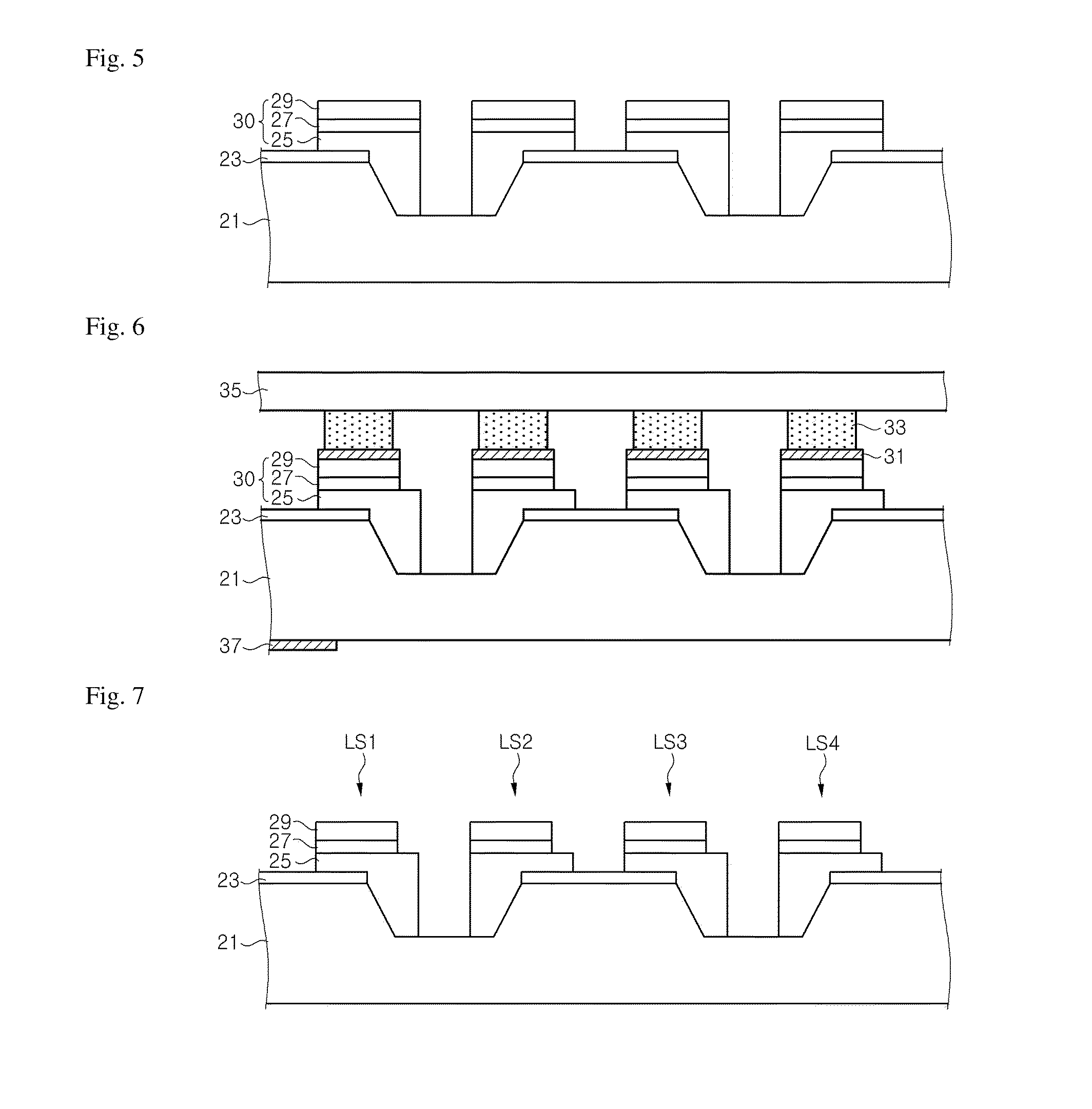
[0059]Referring to FIG. 6, reflective metal layers 31 are formed on the light emitting cells 30, respectively. The reflective metal layer 31 may be formed, for example of Ag or Al. Further, the reflective metal layer 31 may be formed on a portion of the light emitting cell 30, is and a protective metal layer (not shown) may be formed to cover the reflective metal layer 31.

[0060]A second substrate 35 is bonded to the reflective metal layer 31 through bumps 33. The second substrate 35 may be a submount substrate, for example. The second substrate 35 may have an electric circuit therein. The substrate 21 may be a conductive silicon carbide substrate, and an electrode pad 37 may be formed under a lower surface of the substrate 21. Accordingly, there is provided a flip chip having the non-polar light emitt...

second embodiment

[0061]FIG. 7, FIG. 8, FIG. 9, and FIG. 10 are sectional views illustrating a method of fabricating a light emitting device having a plurality of non-polar light emitting cells according to the present invention.

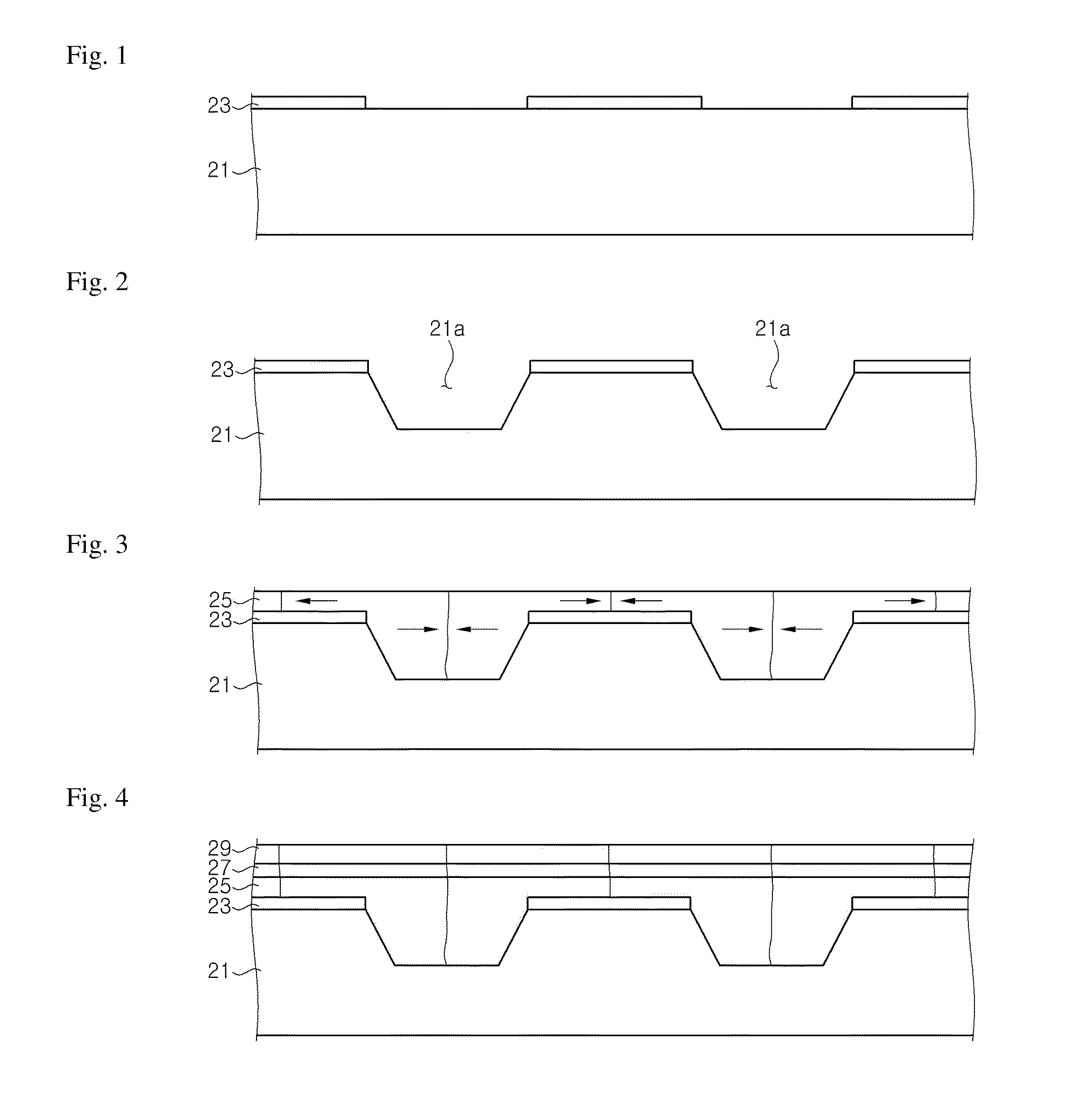
[0062]Referring to FIG. 7, nitride semiconductor layers 25, 27 and 29 are grown on a substrate 21 as described with reference to FIG. 1, FIG. 2, FIG. 3, and FIG. 4. Then, the nitride semiconductor layers 25, 27 and 29 are etched to form light emitting cells LS1, LS2, LS3 and LS4 separated from one another. The first conductive-type nitride semiconductor layer 25 is partially exposed by removing portions of the second conductive-type nitride semiconductor layer 29 and the active layer 27. That is, each of the light emitting cells LS1, LS2, LS3 and LS4 comprises the first conductive-type nitride semiconductor layer 25, the second conductive-type nitride semiconductor layer 29 positioned on one region of the first conductive-type nitride semiconductor layer 25, and the active la...

third embodiment

[0067]FIG. 11 is a sectional view illustrating a method of fabricating a light emitting device having a plurality of non-polar light emitting cells LS1, LS2, LS3 and LS4 according to the present invention.

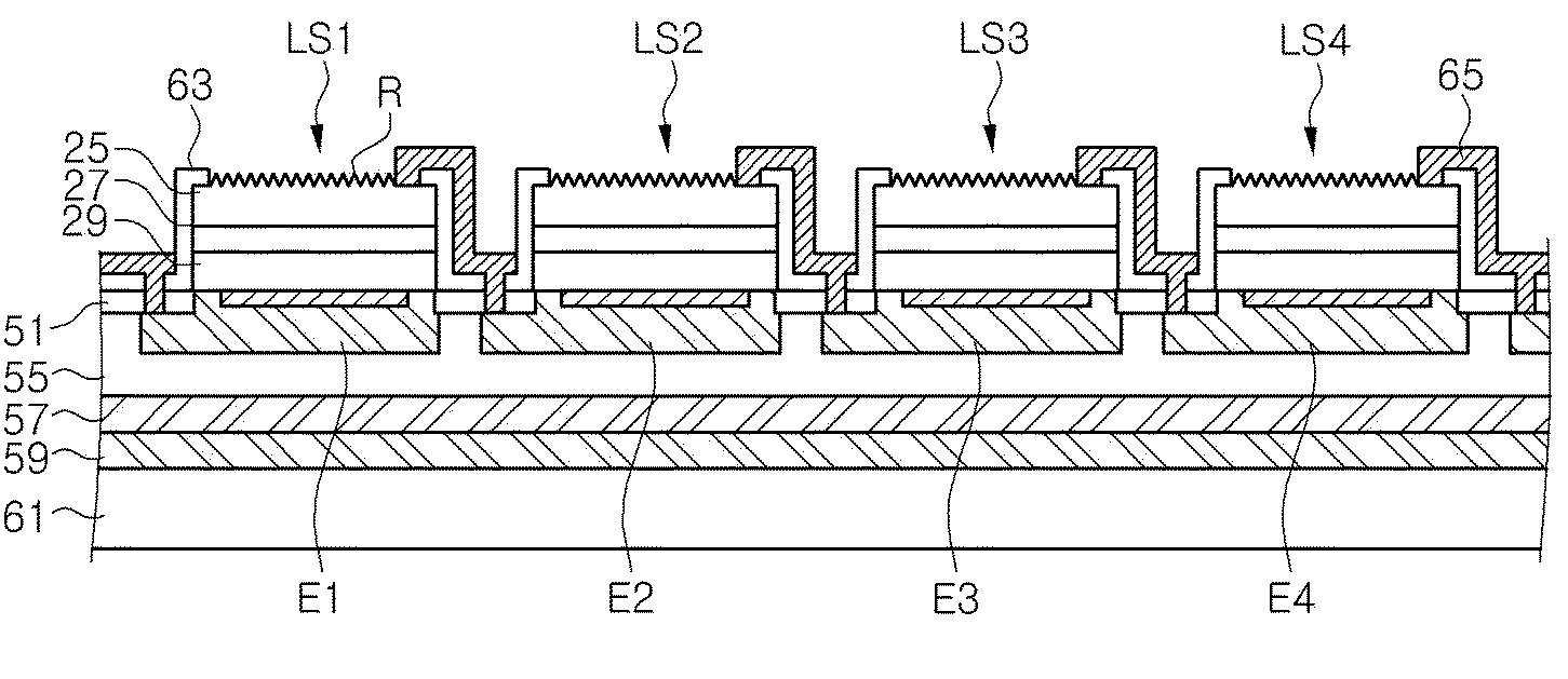
[0068]Referring to FIG. 11, after the wires 47 of FIG. 10 are formed, an interlayer insulating layer 49 is formed to cover the light emitting cells LS1, LS2, LS3 and LS4. The interlayer insulating layer 49 prevents the light emitting cells LS1, LS2, LS3 and LS4 from being short-circuited. A second substrate 50 is bonded to the interlayer insulating layer 49.

[0069]The second substrate 50 may be a submount substrate, and accordingly, there may be provided a flip-chip light emitting device. The submount substrate may have electrode pads, and pads (not shown) for supplying power to the light emitting cells LS1, LS2, LS3 and LS4 may be electrically connected to the electrode pads on the submount substrate through the interlayer insulating layer 49. In this case, light emitted from the l...


PUM


Abstract

Disclosed are a light emitting device having a plurality of non-polar light emitting cells and a method of fabricating the same. This method comprises preparing a first substrate of sapphire or silicon carbide having an upper surface with an r-plane, an a-plane or an m-plane. The first substrate has stripe-shaped anti-growth patterns on the upper surface thereof, and recess regions having sidewalls of a c-plane between the anti-growth patterns. Nitride semiconductor layers are grown on the substrate having the recess regions, and the nitride semiconductor layers are patterned to form the light emitting cells separated from one another. Accordingly, there is provided a light emitting device having non-polar light emitting cells with excellent crystal quality.

Description

CROSS REFERENCE TO RELATED APPLICATION[0001]This application claims priority from and the benefit of Korean Patent Application No. 10-2008-0138422, filed on Dec. 31, 2008, which is hereby incorporated by reference for all purposes as if fully set forth herein.BACKGROUND OF THE INVENTION[0002]1. Field of the Invention[0003]Exemplary embodiments of the present invention relate to a light emitting device and a method of fabricating the same, and more particularly, to a light emitting device having a plurality of non-polar light emitting cells and a method of fabricating the same.[0004]2. Discussion of the Background[0005]GaN-based light emitting diodes (LEDs) are widely used for displays and backlights. Further, LEDs have less electric power consumption and a longer lifespan as compared with conventional light bulbs or fluorescent lamps, so that the LEDs have been substituted for conventional incandescent bulbs and fluorescent lamps and their application areas have been expanded to the...

Claims


Application Information

Patent Timeline
Patent Type & Authority Applications(United States)
IPC IPC(8): H01L33/00H01L21/30
CPCH01L27/156H01L33/007
Inventor SEO, WON CHEOLKIM, KWANG CHOONGYE, KYUNG HEE
Owner SEOUL VIOSYS CO LTD
Why Eureka
Try Eureka