Oscillation device

a technology of oscillating device and oscillating axis, which is applied in the direction of optical radiation measurement, pulse technique, instruments, etc., to achieve the effect of high-speed information communication

Inactive Publication Date: 2010-07-01
CANON KK
View PDF24 Cites 6 Cited by
  • Summary
  • Abstract
  • Description
  • Claims
  • Application Information

AI Technical Summary

Benefits of technology

[0011]Followed by this, the oscillation device of the present invention can be effectively applied particularly in the field of millimeter wave and terahertz wave, e.g., to spectrum inspection and identification of material based thereon used in biosensing, as well as high speed information communication.

Problems solved by technology

However, the configuration using temperature adjustment for allowing oscillation wavelength to be variable in the known long wavelength laser has problems in connection with two points as described below.

Method used


Image

  • Oscillation device
  • Oscillation device
  • Oscillation device

Examples


example 1

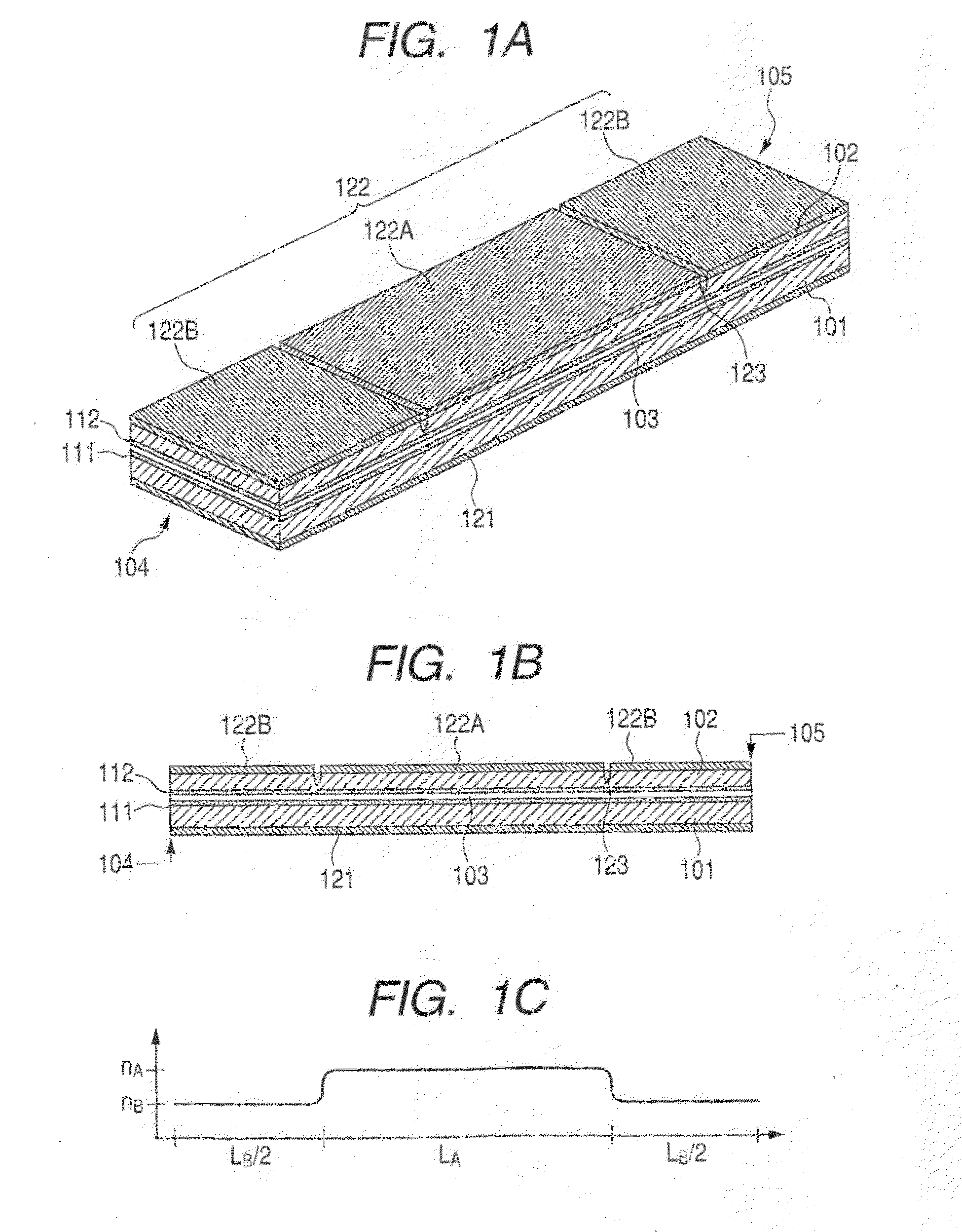
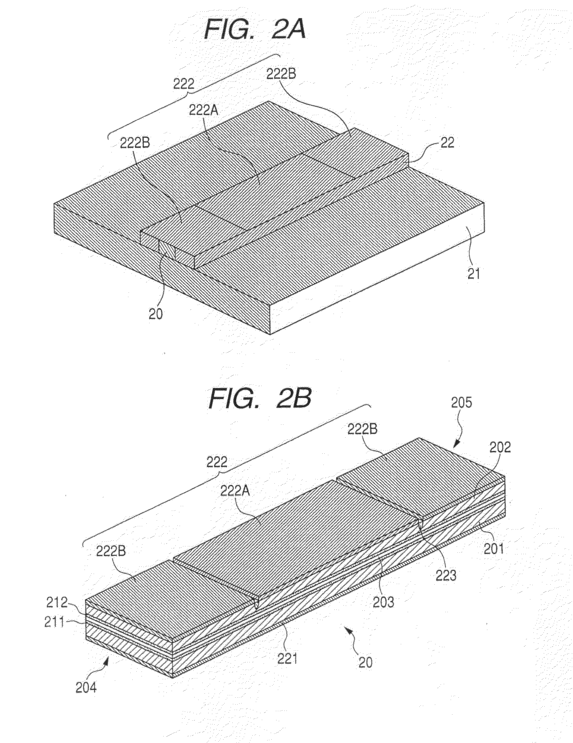
[0043]FIGS. 2A and 2B illustrate a first example of an oscillation device to which the present invention is applied. FIG. 2B illustrates, in an enlarged manner, a device body 20 illustrated in FIG. 2A. In this example, a gain medium is a resonant tunneling diode (RTD) based on photon-assisted tunneling. Gain produced in the RTD is observed as negative resistance in DC. In this case, it is considered that the gain broadly extends from millimeter wave band up to terahertz band. Accordingly, the RTD is a desirable example as a gain medium forming an oscillation device to which the present invention can be applied.

[0044]In FIG. 2B, a gain medium 203 is an RTD, and is of the configuration in which three barrier layers are used like spacer layer / barrier layer / well layer / barrier layer / well layer / barrier layer / spacer layer, for example. In order to realize this configuration, lattice-matched InGaAs may be used on InP substrate as well layer, and lattice-matched InAlAs or non-matched AlAs ma...

example 2

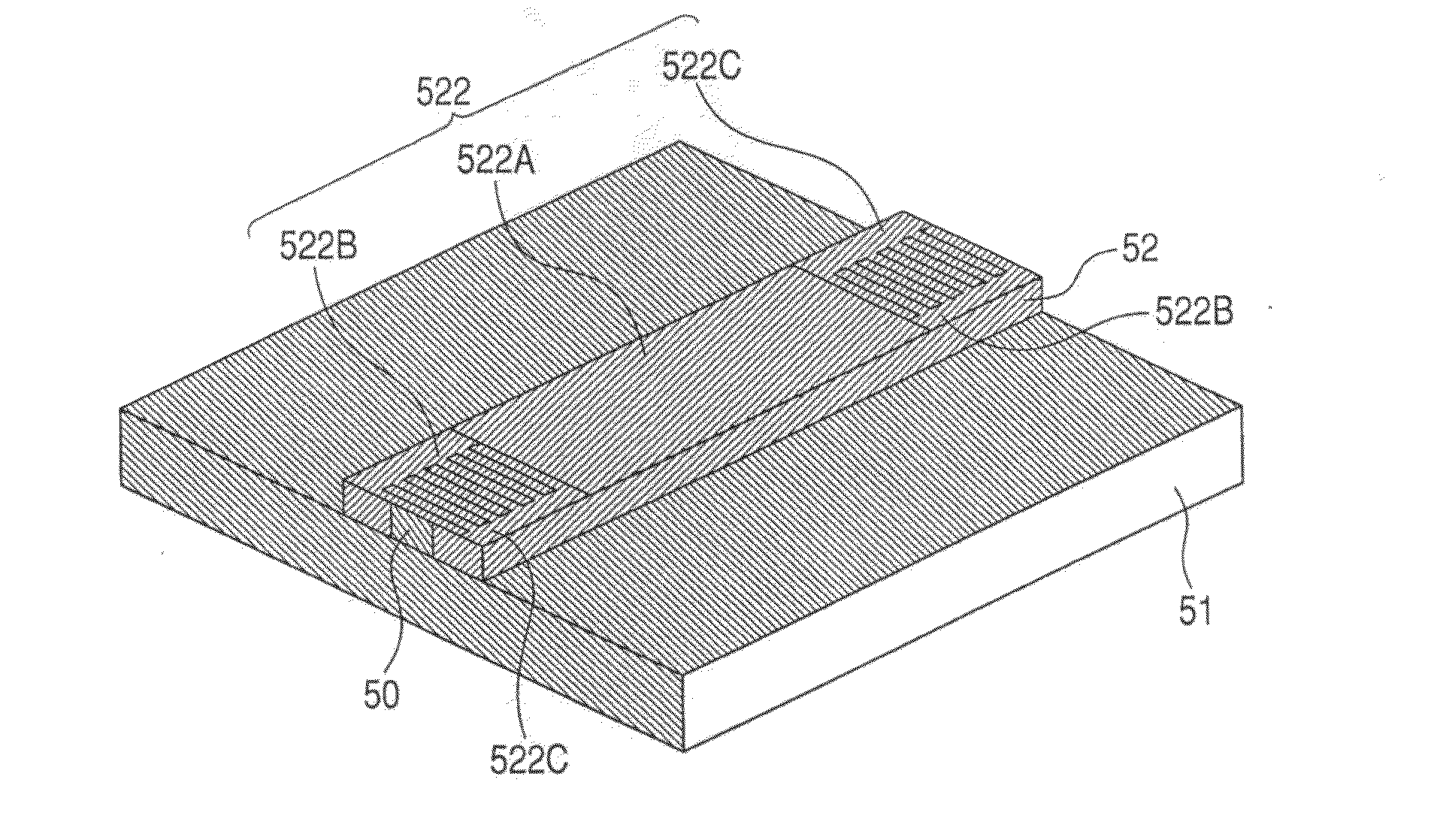
[0059]FIGS. 5A and 5B illustrate the configuration of the second example of an oscillation device to which the present invention is applied. FIG. 5B shows, in an enlarged manner, the device body in FIG. 5A. In this example, the cavity structure uses DBR. Since the cavity structure having wavelength selectivity is employed as the cavity structure differently from Example 1, mode hopping becomes difficult to take place. Accordingly, as cavity structure forming the oscillation device to which the present invention can be applied, this example is a more desirable example.

[0060]In FIG. 5B, an RTD on the same InP substrate as that of Example 1 is used as a gain medium 503. Electrical contacts 511 and 512 are configured so as to include a semiconductor film of n-InGaAs (thickness 50 nm) having electron concentration of 1×1018 cm−3, and negative permittivity media 501, 502 are configured so as to include a semiconductor film of n-InGaAs (thickness 100 nm) having electron concentration of 1×...

example 3

[0067]FIGS. 6A and 6B illustrate the configuration of an oscillation device of the third example to which the present invention is applied. FIG. 6B illustrates, in an enlarged manner, a device body 60 in FIG. 6A. In the present example, a gain medium is a resonant inter-band tunneling diode (RITD) based on photon-assisted tunneling. The RITD has a gain of millimeter wave band utilizing the photon-assisted tunneling. Accordingly, there is disclosed a modified example of a gain medium forming an oscillation device to which the present invention can be applied.

[0068]In FIG. 6B, a gain medium 603 is RITD, and is of the configuration using Type II hetero-junction, e.g., as in the case of n type 8 doped part / spacer layer / Type II spacer layer / p-type 8 doped part / Type II p-type layer. In connection with these components, lattice-matched Si may be used on an Si substrate as a spacer layer, and SiGe which is non-matched and serves as Type II hetero-junctioned to Si may be used as a Type II sp...


PUM


Abstract

To provide an oscillation device having a long oscillation wavelength in which wavelength variable width is relatively broad and wavelength sweep rate is relatively high. An oscillation device includes a gain medium having a gain with respect to an electromagnetic wave to be oscillated, cavity structures for resonating the electromagnetic wave, and energy injection means and for injecting pumping energy into the gain medium. The gain medium is sandwiched between a first negative permittivity medium and a second magnetic permittivity medium each of which real part of permittivity with respect to the electromagnetic wave is negative. Electric field application means is provided for at least one of the first negative permittivity medium and the second negative permittivity medium to apply an electric field for changing a depletion region formed at a boundary part with the gain medium.

Description

TECHNICAL FIELD[0001]The present invention relates to an oscillation device including a gain medium sandwiched between negative permittivity media of which real part of permittivity with respect to an electromagnetic wave is negative. In particular, the present invention relates to a current injection type oscillation device including a waveguide through which surface plasmon with an electromagnetic wave having a frequency within a frequency region from 30 GHz to 30 THz (called millimeter wave and terahertz wave, particularly a region near 30 GHz and a region near 30 THz are respectively called millimeter wave band and terahertz band in this specification) is propagated, and serving to change the depletion region by applying an electric field through electric field control means to allow oscillation wavelength to be variable.BACKGROUND ART[0002]A new type of semiconductor laser called quantum cascade laser which operates based on transition of carriers between energy levels of carri...

Claims


Application Information

Patent Timeline
Patent Type & Authority Applications(United States)
IPC IPC(8): H03B7/08
CPCB82Y20/00H01S1/02H01S5/06255H01S5/06256H01S5/2213H01S5/227H01S5/3027H01S5/3031H01S5/3402H01S5/3422
Inventor SEKIGUCHI, RYOTAOUCHI, TOSHIHIKO
Owner CANON KK
Why Eureka
Try Eureka