Composite substrate and method for forming metal pattern

a technology of composite substrate and metal pattern, which is applied in the field of composite substrate and a method for forming metal pattern, can solve the problems of inability to form desired resist pattern, inability to form desired metal pattern, and inability to expose a large amount of photoresist to light, so as to achieve high degree of precision, higher thermal expansion coefficient, and high thermal expansion coefficient

Active Publication Date: 2010-07-01
NGK INSULATORS LTD
View PDF5 Cites 6 Cited by
  • Summary
  • Abstract
  • Description
  • Claims
  • Application Information

AI Technical Summary

Benefits of technology

[0022]In a composite substrate according to the second aspect of the present invention, when a desired metal pattern is formed on a surface of a piezoelectric substrate by a lift-off process using photolithography, light passing through a photoresist passes through the piezoelectric substrate, a first organic adhesive layer, and a supporting substrate in this order and is absorbed by a second organic adhesive layer. A portion of the photoresist on the back side of a photomask is therefore not exposed to light. As in a composite substrate according to the first aspect of the present invention, therefore, a desired metal pattern can be formed with a high degree of precision by a lift-off process using photolithography. The second organic adhesive layer may be formed of a material in which a light-absorbing component is added to an adhesive composition.
[0023]A composite substr...

Problems solved by technology

The portion of the photoresist is therefore undesirably exposed to light, and a desired resist pattern cannot be formed.
Thus, a desired metal pattern also cannot be formed.
Furtherm...

Method used


Image

  • Composite substrate and method for forming metal pattern
  • Composite substrate and method for forming metal pattern
  • Composite substrate and method for forming metal pattern

Examples


example 1

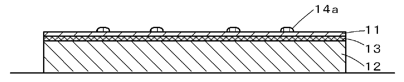
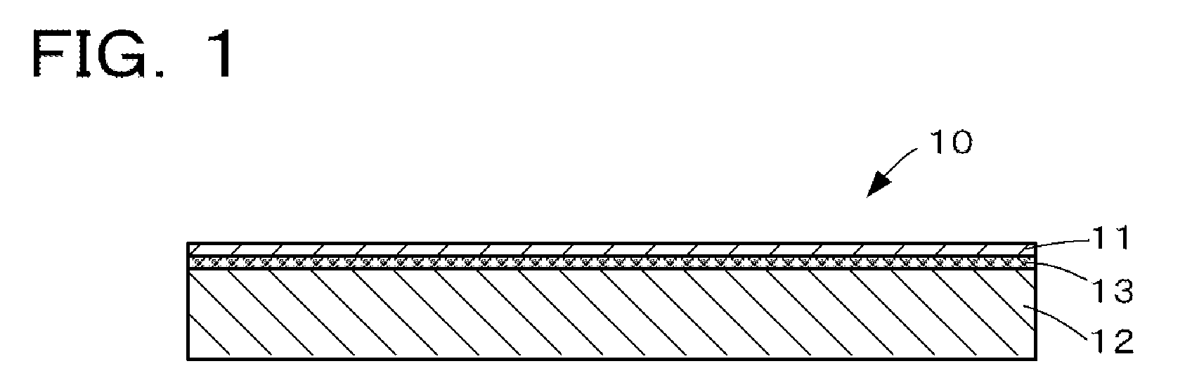
[0048]As Example 1, a composite substrate 10 illustrated in FIG. 1 was fabricated, and a metal pattern was formed by a lift-off process using photolithography.

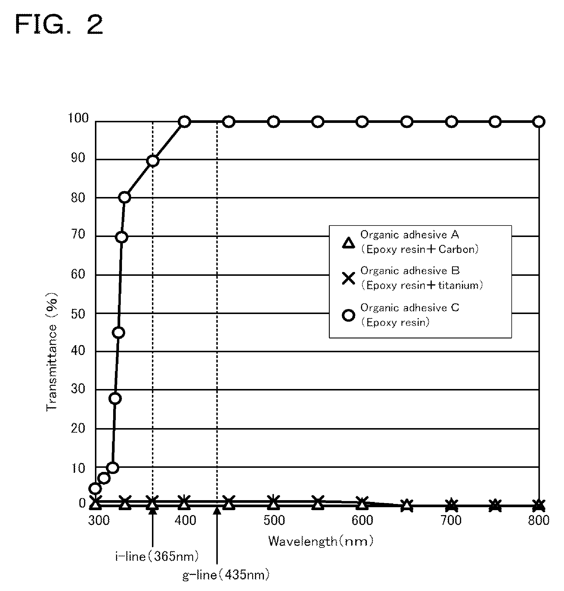
[0049]More specifically, first, a lithium tantalate substrate (hereinafter referred to as an LT substrate) having a thickness of 250 μm and a diameter of 100 mm, which served as a piezoelectric substrate 11, and a borosilicate glass substrate having a thickness of 250 μm and a diameter of 100 mm, which served as a supporting substrate 12, were prepared. The LT substrate was a 42° Y-cut H-propagation LT substrate, in which H denotes the propagation direction of a surface acoustic wave (SAW), and the cut angle was a rotated Y-cut. Subsequently, the above-mentioned organic adhesive A was applied to a surface of the borosilicate glass substrate by spin coating. The back side of the LT substrate was bonded to the surface of the borosilicate glass substrate on which the organic adhesive A was applied. Heating at 160° C. produced a l...

example 2

[0051]A composite substrate 10 was fabricated, and a metal pattern was completed, as in Example 1 except that the material of the supporting substrate 12 was silicon instead of borosilicate glass. Measuring the widths of the metal pattern thus completed at 100 positions, the metal pattern had a width of 0.5±0.05 μm with a standard deviation σ of 0.02 μm.


PUM

PropertyMeasurementUnit
Wavelengthaaaaaaaaaa
Transparencyaaaaaaaaaa
Lightaaaaaaaaaa

Abstract

A composite substrate 10 is a composite substrate in which a piezoelectric substrate 11 that is transparent to light used for photolithography and a supporting substrate 12 for supporting the piezoelectric substrate 11 are bonded together via an organic adhesive layer 13. At least one of the supporting substrate 12 and the organic adhesive layer 13 of the composite substrate 10 can absorb light used for photolithography.

Description

BACKGROUND OF THE INVENTION[0001]1. Field of the Invention[0002]The present invention relates to a composite substrate and a method for forming metal pattern.[0003]2. Description of the Related Art[0004]It is known that the formation of a desired metal pattern on a surface of a substrate by photolithography involves forming a resist pattern using a photoresist, forming a thin metal film layer on the surface on which the resist pattern is formed, and then removing the resist to form the desired metal pattern. This method is generally referred to as a lift-off process. For example, in a method for forming a thin metal film pattern described in Patent Document 1, after a resist pattern is formed on a substrate, a thin metal film layer is formed by sputtering. After immersion in a stripping solution for the resist pattern, an ultrasonic wave is applied to remove the resist pattern and an unnecessary portion of the thin metal film layer disposed on the resist pattern.[Patent Documents][0...

Claims


Application Information

Patent Timeline
IPC IPC(8): G03F7/20B32B27/38B32B27/06B32B27/36B32B27/04B32B33/00B32B15/08H03H3/08H01L41/047H01L41/09H01L41/18H01L41/22H01L41/29H03H9/25
CPCH01L41/29H03H3/08H03H9/02574H01L41/313Y10T428/31518Y10T428/31515Y10T428/31786Y10T428/31616Y10T428/2804Y10T428/2848H10N30/06H10N30/073
Inventor SUZUKI, KENJIIWASAKI, YASUNORIYOSHINO, TAKASHI
Owner NGK INSULATORS LTD
Why Eureka
Try Eureka