Solid printed circuit board and method of manufacturing the same

a printed circuit board and solid-state technology, applied in the direction of printed element electric connection formation, conductive pattern formation, non-metallic protective coating application, etc., can solve the problems of reducing preventing the complete interconnection of the circuit board with a lot of pins, etc., to achieve the effect of increasing the wiring density of the circuit board and low profil

Inactive Publication Date: 2010-07-08
PANASONIC CORP
View PDF2 Cites 47 Cited by
  • Summary
  • Abstract
  • Description
  • Claims
  • Application Information

AI Technical Summary

Benefits of technology

[0007]The present invention relates to a solid printed circuit board including plural printed circuit boards having different shapes and having wirings thereon, and a bonding layer bonding these printed circuit boards. The bonding layer is made of insulating material containing resin. A through-hole is provided in the bonding layer. The bonding layer includes a via-conductor made of conductive paste filling the through-hole. This structure connects between the circuit boards having pins while increasing the wiring density within the circuit boards. The circuit board has a recess to have an electronic component mounted therein, thus providing the printed circuit board with a low profile.

Problems solved by technology

This problem prevents complete interconnections between circuit boards having a lot of pins, and reduces a wiring density within the circuit boards.

Method used


Image

  • Solid printed circuit board and method of manufacturing the same
  • Solid printed circuit board and method of manufacturing the same
  • Solid printed circuit board and method of manufacturing the same

Examples


exemplary embodiment 1

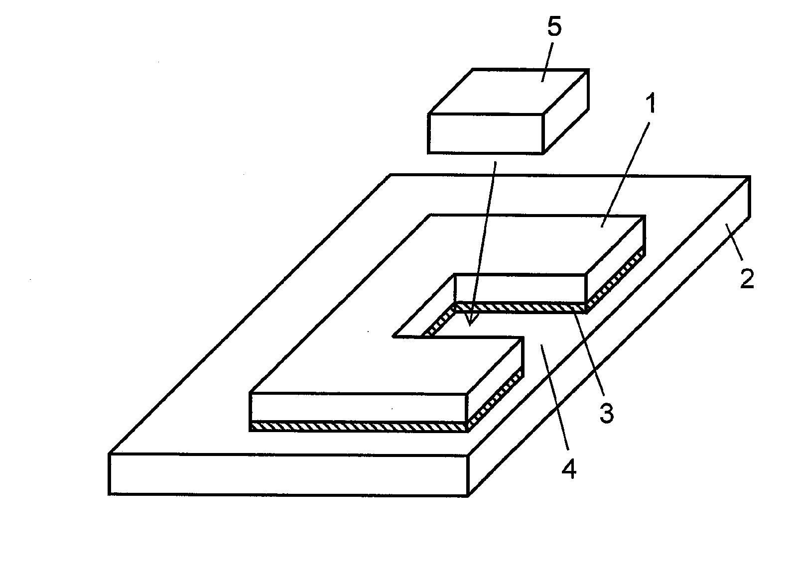
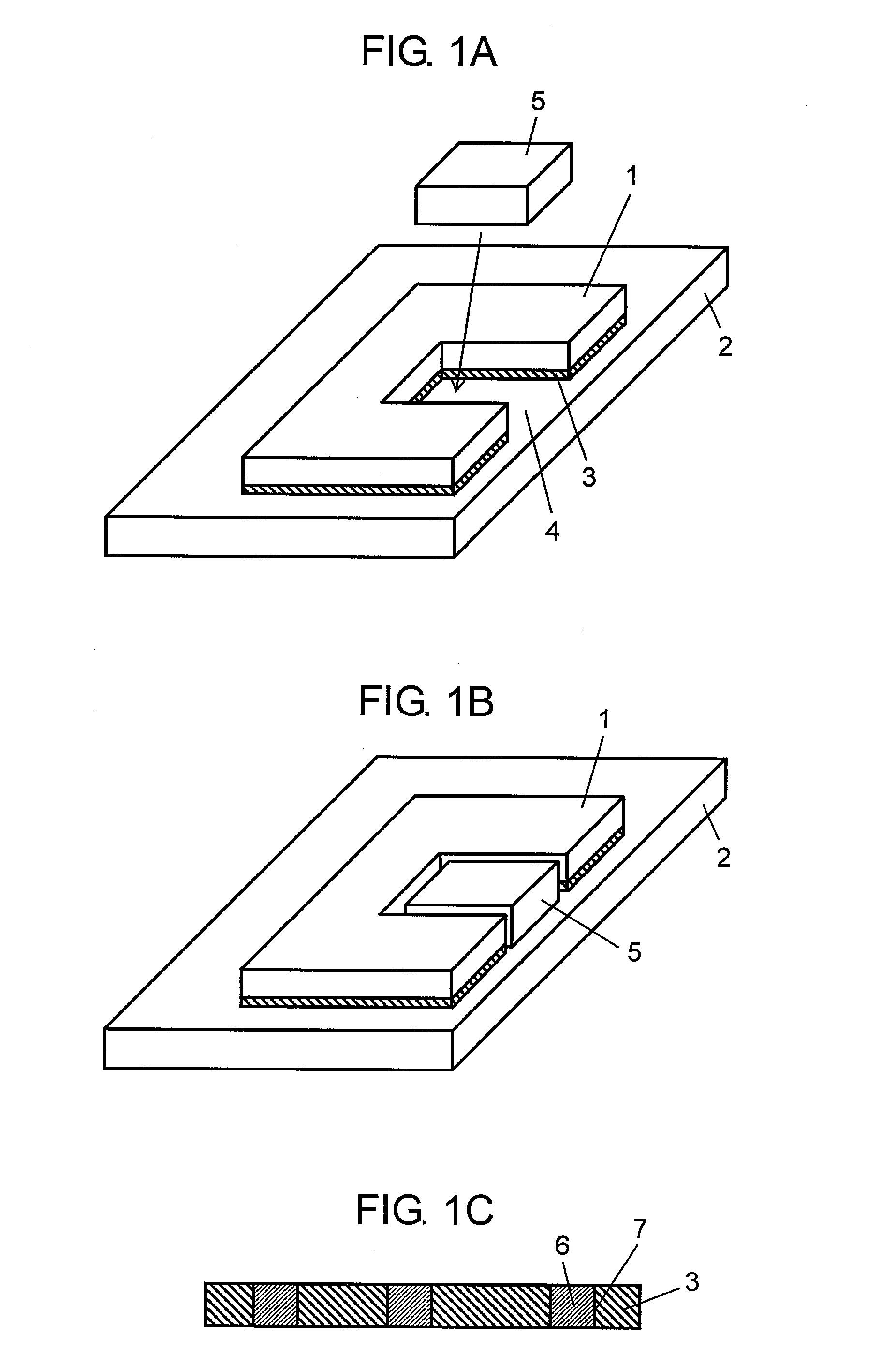
[0081]Exemplary Embodiment 1 of the present invention will be described below with reference to accompanying drawings. FIGS. 1A and 1B are perspective views of a solid printed circuit board according to this embodiment. The solid printed circuit board according to this embodiment includes upper printed circuit board 1 and lower printed circuit board 2 having different shapes from each other and having wirings formed thereon, and bonding layer 3. Since upper printed circuit board 1 and lower printed circuit board 2 having different shapes, the circuit boards form recess 4, a cavity, as shown in FIG. 1A. Bonding layer 3 has a thickness ranging preferably from 30 to 300 μm. Bonding layer 3 having a thickness less than 30 μm may prevent a wiring from being embedded preferably. Bonding layer 3 having a thickness exceeding 300 μm prevents a via-conductor from having a small diameter in order to maintain an aspect ratio of the via-conductor, and may reduce reliability of connection.

[0082]F...

exemplary embodiment 2

[0100]Exemplary Embodiment 2 of this invention will be described with reference to accompanying drawings. A basic structure of this embodiment is similar to that of Embodiment 1 shown in FIG. 1A Solid printed circuit board 16 according to this embodiment will be described in detail with reference to FIG. 8. FIG. 8 is a sectional view of solid printed circuit board 16 according to this embodiment. According to this exemplary embodiment, solder resist 14 is formed on a peripheral edge of the bonding layer 3, as shown in FIG. 8. Bonding layer 3 of the solid printed circuit board has an area smaller than that of upper printed circuit board 1, and solder resist 14 on the peripheral edge of bonding layer 3 protrudes from a surface of lower printed circuit board 2. Bonding layer 3 has the area smaller than that of upper printed circuit board 1, and provides a space for storing flow-out resin 15 flowing from bonding layer 3 produced in the process of hot press. Solder resist 14 protruding o...

exemplary embodiment 3

[0115]Exemplary Embodiment 3 of this invention will be described below. FIG. 13A is a perspective view of a solid printed circuit board according to Exemplary Embodiment 3 of this invention. FIG. 13B is a sectional view of the solid printed circuit board according to Embodiment 3. FIG. 13C is a sectional view of a bonding layer of the solid printed circuit board according to Embodiment 3. The structure of this embodiment is generally analogous to that shown in FIGS. 7A and 7B according to the previous embodiment. According to this embodiment, metal film 17 covers upper printed circuit board 1 and recesses 4, as shown in FIGS. 13A and 13B. Metal film 17 covering recesses 4 can protect wirings and electronic components located inside recesses 4 from electromagnetic noises and electrostatic noises from the outside. The metal film may be connected with upper printed circuit board 1 to provide partial shielding. Recesses 4 allow the metal films to be formed on arbitrary positions, thus a...


PUM

PropertyMeasurementUnit
thicknessaaaaaaaaaa
thicknessaaaaaaaaaa
thicknessaaaaaaaaaa

Abstract

A solid printed circuit board is manufactured by bonding upper and lower printed circuit boards having different shapes and provided with wirings formed on surfaces thereof. A bonding layer is made of insulating material containing thermosetting resin and inorganic filler dispersed therein, and has a via-conductor made of conductive paste filling a through-hole perforated in a predetermined position of the bonding layer. This circuit board provides a packaging configuration achieving small size and thickness and three-dimensional mounting suitable for semiconductors of high performance and multiple-pin structure.

Description

[0001]This application is a U.S. National Phase Application of PCT International Application PCT / JP2008 / 001323.TECHNICAL FIELD[0002]The present invention relates to a solid printed circuit board used for various electronic apparatuses, such as personal computers, portable telephones, and video cameras, and to a method of manufacturing the circuit board.BACKGROUND ART[0003]Portable products, such as personal computers, digital cameras, and portable phones, have recently prevailed and have been demanded to have small sizes, low profiles, small weights, high densities, and multifunction. According to this demand, semiconductors have their packages having small sizes, low profiles, and three-dimensional mounting. A cavity board is known as a method of easily providing a semiconductor package having a low profile and three-dimensional mounting.[0004]A conventional cavity board will be described below with reference to FIG. 24. FIG. 24 is a sectional view of a conventional solid printed c...

Claims


Application Information

Patent Timeline
Patent Type & Authority Applications(United States)
IPC IPC(8): H05K1/00H05K1/09H05K3/42H05K3/46
CPCH05K1/183H05K1/189H05K3/28H05K3/3452H05K3/4069H05K3/4614H05K3/4691H05K3/4694H05K3/4697H05K2201/09145H05K2201/09845H05K2201/09909H05K2201/09972H05K2201/10378H05K2201/10674H05K2201/2018H05K2203/061Y10T29/49124Y10T29/49165Y10T29/49155
Inventor NAKAMURA, TADASHIECHIGO, FUMIOKITA, TAKAYUKIFUKASAWA, KOTAHIRAI, SHOGO
Owner PANASONIC CORP
Why Eureka
Try Eureka