Process for producing magnetic device, apparatus for producing magnetic device, and magnetic device

a technology for producing magnetic devices and magnetic devices, which is applied in the field of manufacturing magnetic devices, apparatus for manufacturing magnetic devices, and magnetic devices, and can solve the problems of large variations in the composition and film thickness of the antiferromagnetic layer within the plane surface of the substrate, and significantly deteriorating the magnetic characteristics of the devi

Inactive Publication Date: 2010-07-08
ULVAC INC
View PDF6 Cites 8 Cited by
  • Summary
  • Abstract
  • Description
  • Claims
  • Application Information

AI Technical Summary

Benefits of technology

[0017]The present invention provides a method for manufacturing a magnetic device, an apparatus for manufacturing a magnetic device, and a magnetic device manufactured b

Problems solved by technology

As a result, the high-pressure process causes large variations in the composition and film thickness of the antiferromagnetic layer within the plane surface of the substrate.
In a magnetic device that requires thickness uniformity and allows for each layer to have a thickness variation range of one nanometer or less, variations in the composition and film thickness of the antiferromagnetic layer would significantly deteriorate the magnetic characteristics of the device.

Method used


Image

  • Process for producing magnetic device, apparatus for producing magnetic device, and magnetic device
  • Process for producing magnetic device, apparatus for producing magnetic device, and magnetic device
  • Process for producing magnetic device, apparatus for producing magnetic device, and magnetic device

Examples


example

[0059]An example will now be used to describe the present invention.

[0060]First, a silicon wafer having a diameter of 200 mm was used as a substrate. A film formation process was performed on the substrate S by the manufacturing apparatus 10 to obtain a superimposed film of Ta (5 nm) / Ru (20 nm) / MnIr (10 nm) / CoFe (4 nm) / Ru (1 nm) / Ta (2 nm).

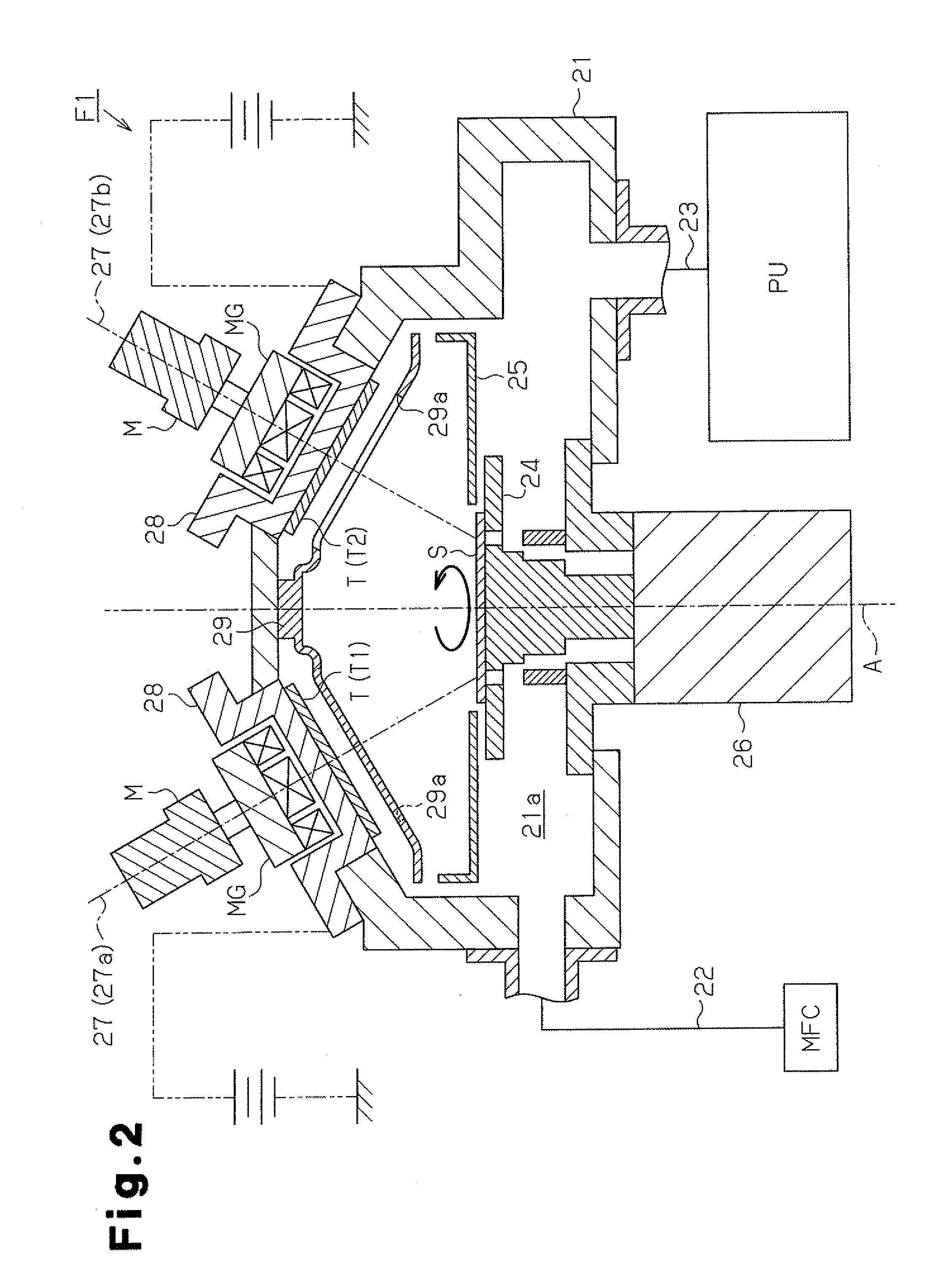
[0061]In detail, the antiferromagnetic layer chamber F1 was used to superimpose a Ta film having a thickness of 5 nm and an Ru film having a thickness of 20 nm, and then an MnIr film having a thickness of 10 nm was formed to obtain the antiferromagnetic layer. An alloy target of which composition was Mn77Ir23 and having a diameter of 125 mm was used as the second target T2. The distance between the substrate S and the target T was set as 200 mm in the normal direction of each target T. Further, Kr was used as the processing gas.

[0062]Next, the fixed layer chamber F2 and the free layer chamber F4 were used to form a CO70Fe30 film having a thickness ...


PUM

PropertyMeasurementUnit
Temperatureaaaaaaaaaa
Pressureaaaaaaaaaa

Abstract

A magnetic device manufacturing apparatus that increases the unidirectional anisotropy constant (JK). A substrate (S) is placed in a substrate holder (24) in a film formation area (21a), the substrate (S) is heated to a predetermined temperature, and the processing pressure is reduced to 0.1 (Pa) or lower. A target (T2) of which a main component is an element forming the antiferromagnetic layer is sputtered with at least either one of Kr and Xe to form an antiferromagnetic layer. The antiferromagnetic layer includes an L12 ordered phase expressed by compositional formula Mn100-X-MX (where M is at least one element selected from the group consisting of Ru, Rh, Ir, and Pt, and X is 20(atom %)≦X≦30(atom %)).

Description

TECHNICAL FIELD[0001]The present invention relates to a method for manufacturing a magnetic device, an apparatus for manufacturing a magnetic device, and a magnetic device.BACKGROUND ART[0002]Magnetoresistance elements implementing a giant magnetoresistance (GMR) effect or a tunnel magnetoresistance (TMR) effect has a superior magnetoresistance change rate and is thus used in magnetic devices, such as magnetic sensors, magnetic reproduction heads, and magnetic memories.[0003]A magnetoresistance element, which has an artificial lattice structure of about six to fifteen layers, includes a free layer having a rotatable spontaneous magnetization direction, a fixed layer having a fixed spontaneous magnetization direction, a non-magnetic layer arranged between the fixed layer and free layer, and an antiferromagnetic layer that induces unidirectional anisotropy relative to the fixed layer.[0004]Known antiferromagnetic layers include a manganese iridium (MnIr) thin film and a platinum manga...

Claims


Application Information

Patent Timeline
IPC IPC(8): C23C14/34
CPCB82Y10/00H01F41/18H01L43/12H01L43/08H01L27/228H10B61/22H10N50/01H10N50/10G11B5/39
Inventor IMAKITA, KENICHI
Owner ULVAC INC
Why Eureka
Try Eureka