Copper delafossite transparent p-type semiconductor thin film devices

a technology of transparent p-type semiconductor and copper delafossite, which is applied in the manufacture of copper delafossite transparent p-type semiconductor materials, sustainable manufacturing/processing, electrolytic capacitors, etc., can solve the problems of limiting the use of these cells, limiting the stability of these cells, and evaporating and leaking liquid electrolyte from the cell

Inactive Publication Date: 2010-07-15
APPLIED MATERIALS INC
View PDF9 Cites 41 Cited by
  • Summary
  • Abstract
  • Description
  • Claims
  • Application Information

AI Technical Summary

Benefits of technology

[0007]Certain embodiments of the present invention are processes for making Cu delafossite materials including: a low temperature sol-gel process for synthesizing CuBO2 materials; a process which controls the band gap of the CuBO2 material by controlling the particle size; a process for making ultrafine powders of CuBO2 capable of penetrating a dyed porous TiO2 network; a process for forming TiO2—CuBO2 “core-shell” nanoparticles; a process for forming TiO2—CuBO2 “nano-couples”; and a deposition p...

Problems solved by technology

However, all of these oxides are characterized as n-type materials and their use is accordingly limited.
However, a major problem with these DSSCs is the evaporation and possible leakage of the liquid electrolyte from the cell.
This limits the stability of these cells and al...

Method used


Image

  • Copper delafossite transparent p-type semiconductor thin film devices
  • Copper delafossite transparent p-type semiconductor thin film devices
  • Copper delafossite transparent p-type semiconductor thin film devices

Examples


Embodiment Construction

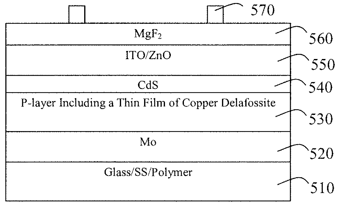
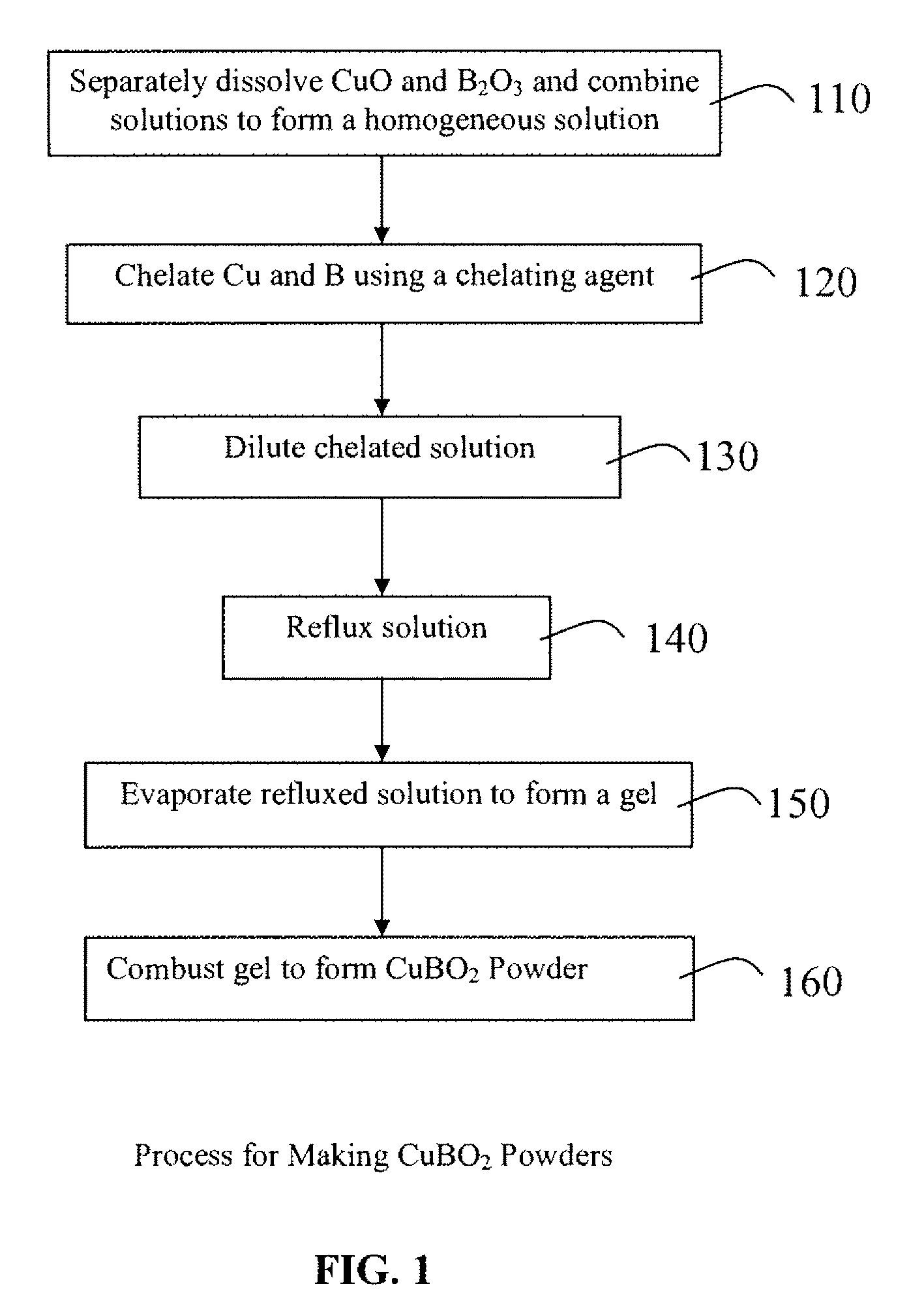
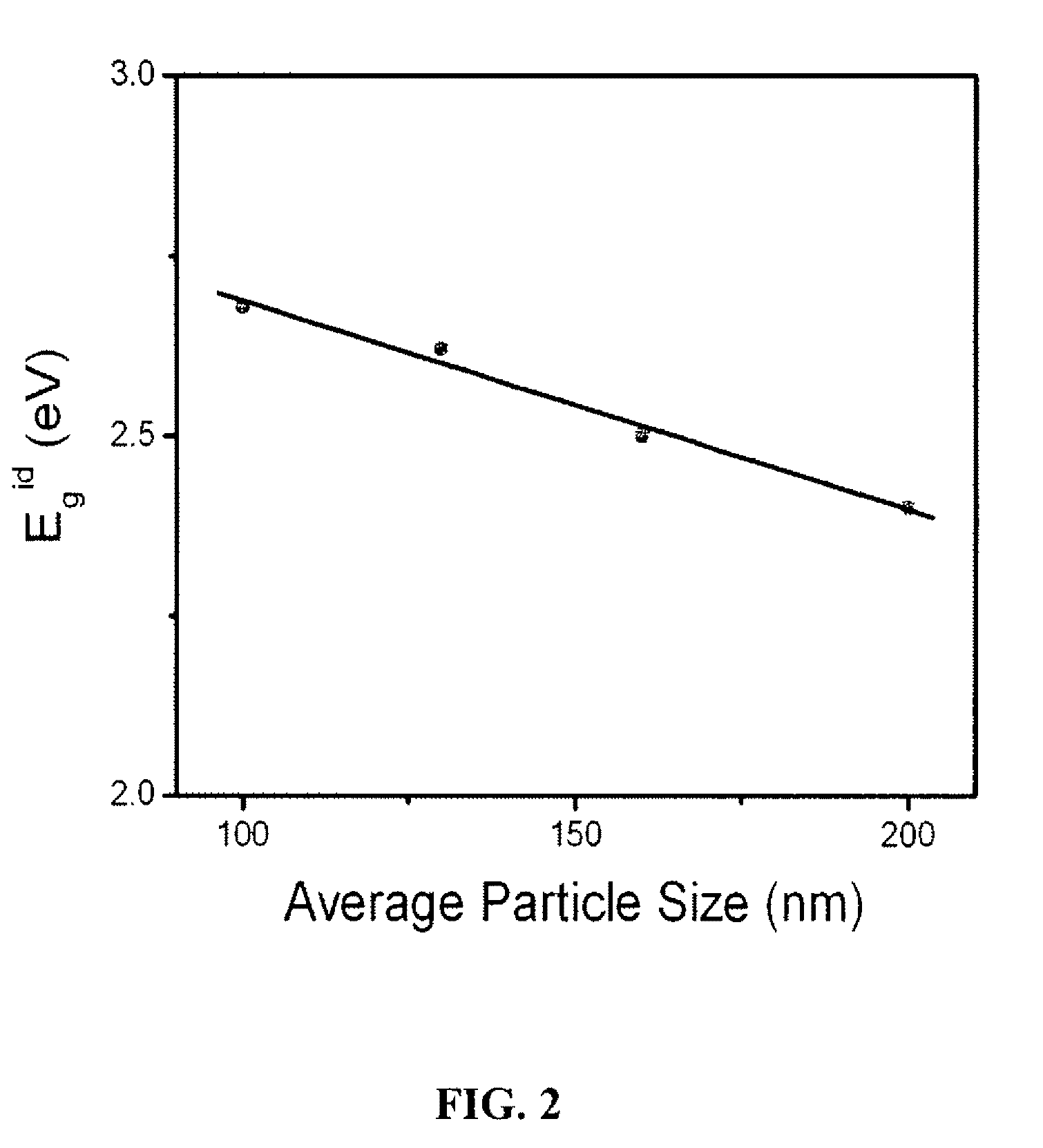
[0032]The present invention will now be described in detail with reference to the drawings, which are provided as illustrative examples of the invention so as to enable those skilled in the art to practice the invention. Notably, the figures and examples below are not meant to limit the scope of the present invention to a single embodiment, but other embodiments are possible by way of interchange of some or all of the described or illustrated elements. Moreover, where certain elements of the present invention can be partially or fully implemented using known components, only those portions of such known components that are necessary for an understanding of the present invention will be described, and detailed descriptions of other portions of such known components will be omitted so as not to obscure the invention. In the present specification, an embodiment showing a singular component should not be considered limiting; rather, the invention is intended to encompass other embodimen...


PUM


Abstract

Methods for fabrication of copper delafossite materials include a low temperature sol-gel process for synthesizing CuBO2 powders, and a pulsed laser deposition (PLD) process for forming thin films of CuBO2, using targets made of the CuBO2 powders. The CuBO2 thin films are optically transparent p-type semiconductor oxide thin films. Devices with CuBO2 thin films include p-type transparent thin film transistors (TTFT) comprising thin film CuBO2 as a channel layer and thin film solar cells with CuBO2 p-layers. Solid state dye sensitized solar cells (SS-DSSC) comprising CuBO2 in various forms, including “core-shell” and “nano-couple” particles, and methods of manufacture, are also described.

Description

CROSS-REFERENCE TO RELATED APPLICATIONS[0001]This application claims the benefit of U.S. Provisional Application Ser. No. 61 / 203,336 filed Dec. 19, 2008, incorporated by reference in its entirety herein.FIELD OF THE INVENTION[0002]The present invention relates to transparent p-type semiconductor materials, more specifically methods of manufacture of copper delafossite transparent p-type semiconductor material and devices comprising said copper delafossite material, including solar cells and transparent thin film transistors.BACKGROUND OF THE INVENTION[0003]Transparent conductive oxides (TCOs), such as doped zinc oxide, indium tin oxide (ITO) and indium molybdenum oxide are widely used as conductive optically transparent electrodes. These oxides exhibit both high electrical conductivity and optical transparency, in the visible spectrum. However, all of these oxides are characterized as n-type materials and their use is accordingly limited. In order to expand the use of TCOs to applic...

Claims


Application Information

Patent Timeline
IPC IPC(8): H01L31/032H01L21/16H01L29/786
CPCH01G9/2031H01L51/4226C25B1/003Y02E10/549Y02E10/542Y02P70/50C25B1/55H10K30/151
Inventor SINGH, KAUSHAL K.NALAMASU, OMKARAMKRISHNA, NETY M.SNURE, MICHAELTIWARI, ASHUTOSH
Owner APPLIED MATERIALS INC
Why Eureka
Try Eureka