Solid-state image capturing apparatus, method for manufacturing the same, and electronic information device

a technology of solid-state image and capturing apparatus, which is applied in the direction of television system scanning details, radioation control devices, television systems, etc., can solve the problems of deterioration of diffusion layer, variance in performance between pixel sections, and difficulty in enhancing the degree of integration in a pixel, so as to achieve the effect of not reducing the resolution of the solid-state image capturing apparatus, not reducing the efficiency of light focusing, and high functionality

Inactive Publication Date: 2010-07-15
SHARP KK
View PDF8 Cites 24 Cited by
  • Summary
  • Abstract
  • Description
  • Claims
  • Application Information

AI Technical Summary

Benefits of technology

[0014]In addition, as shown in FIG. 9, in the conventional solid-state image capturing apparatus disclosed in Reference 1, multi-layered wiring layer 105 functioning as a transfer path are provided on the same side as the light incidence side of a semiconductor substrate 106, wherein the multi-layered wiring layers are provided to transfer signal charges output from pixel sections. As such, in order to focus the light upon a light receiving section, it is necessary to arrange the wiring layer 105 at a location where the wiring layer 105 is not provided directly above the light receiving section. In other words, the location where the wiring layer 105 can be provided is extremely limited. Thus, it is difficult to enhance the degree of integration in a pixel. Further, the more multi-layered wiring layer 105 becomes, the deeper the light receiving sections are located from the light incidence surface. In particular, in order to prevent light that is incident from an oblique direction from being deflected by the wiring layer 105 in a light path, it is necessary to form on-chip microlenses on the wiring layer 105 so as to focus the light upon the light receiving sections in an efficient manner. Therefore, in the conventional solid-state image capturing apparatus 100 disclosed in Reference 1, it is necessary to provide a color-filter forming step and an on-chip microlens forming step in a manufacturing process associated with the optical characteristic that is specific to the solid-state image capturing apparatus 100. Accordingly, a manufacturing step becomes complicated, thus reducing the yield.
[0071]Further, it is possible to eliminate the color-filter forming step and the on-chip microlens forming step that were required in a manufacturing process associated with the optical characteristic specific to a solid-state image capturing apparatus in the conventional method for manufacturing the solid-state image capturing apparatus, and thus it is possible to manufacture the solid-state image capturing apparatus with the same line that is used for another semiconductor device. Therefore, even when another semiconductor device and a solid-state image capturing apparatus are mounted in the same chip module in a mixed manner, it is possible to have an improved conformity in the process and to reduce the cost for manufacturing an electronic information device.

Problems solved by technology

However, the conventional solid-state image capturing apparatus disclosed in Reference 1 has the following problems.
Therefore, it is difficult to enhance the degree of integration in a pixel.
As such, the alignment precision between the light receiving section diffusion layer and the pixel separation diffusion layer deteriorates, which becomes a cause of variance in performance between pixel sections.
In other words, the location where the wiring layer 105 can be provided is extremely limited.
Thus, it is difficult to enhance the degree of integration in a pixel.
Accordingly, a manufacturing step becomes complicated, thus reducing the yield.
In addition, the conventional solid-state image capturing apparatus disclosed in Reference 2 has the following problems.

Method used


Image

  • Solid-state image capturing apparatus, method for manufacturing the same, and electronic information device
  • Solid-state image capturing apparatus, method for manufacturing the same, and electronic information device
  • Solid-state image capturing apparatus, method for manufacturing the same, and electronic information device

Examples


embodiment 1

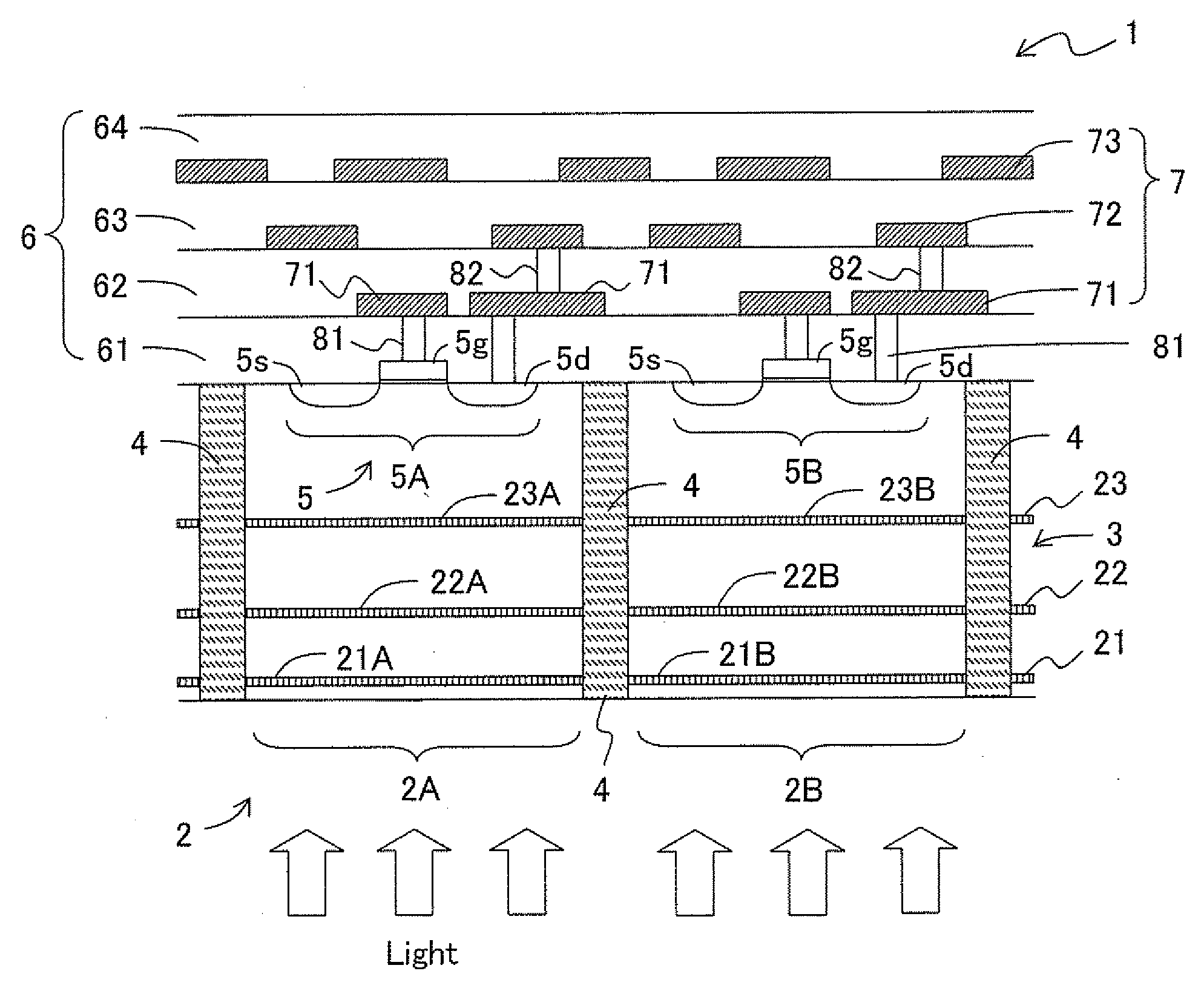
[0109]Embodiment 1 describes a solid-state image capturing apparatus including, in a depth direction of a substrate, a first light receiving section for detecting an electromagnetic wave having a first wavelength band, a second light receiving section for detecting an electromagnetic wave having a second wavelength band, and a third light receiving section for detecting an electromagnetic wave having a third wavelength band, as a plurality of light receiving sections; and a solid-state image capturing apparatus manufacturing method. In this case, three primary colors of red (R), green (G) and blue (B) can be considered as three colors having different wavelength bands of light, for example. Herein, light having the first wavelength band represents blue light, light having the second wavelength band represents green light, and light having the third wavelength band represents red light.

[0110]FIG. 1 is a longitudinal cross-sectional view showing an exemplary essential structure of two...

embodiment 2

[0131]Embodiment 2 describes an example of a preferred size of a solid-state image capturing device and the number of the solid-state image capturing devices to be effectively arranged.

[0132]FIG. 6 is a plane view schematically showing an exemplary essential structure of a solid-state image capturing apparatus 11 according to Embodiment 2 of the present invention.

[0133]In FIG. 6, the solid-state image capturing apparatus 11 according to Embodiment 2 is a CMOS image sensor. In the solid-state image capturing apparatus 11, three row selection signal lines and reset signal lines 12 and three column image signal lines 13 make up one set, and they are arranged to intersect with each other (at right angles). A plurality of solid-state image capturing devices 14 (which correspond to pixel sections 2 in FIG. 1) are repeatedly arranged (in a matrix) according to a sequence at intersections of both signal lines 12 and 13. The row selection signal lines and reset signal lines 12 and the column...

embodiment 3

[0138]Embodiment 3 describes an example of an electronic information device using a solid-state image capturing apparatus according to the present invention as an image input section for an image capturing section thereof.

[0139]FIG. 8 is a block diagram schematically showing an exemplary essential structure of an electronic information device 31 according to Embodiment 3 of the present invention.

[0140]In FIG. 8, the electronic information device 31 according to Embodiment 3 includes: the solid-state image capturing apparatus 1 according to Embodiment 1 or the solid-state image capturing apparatus 11 according to Embodiment 2; a memory section 32 (e.g., recording media) for data-recording a color image signal from the solid-state image capturing apparatus 1 or 11 after a predetermined signal process is performed on the color image signal for recording; a display section 33 functioning as a display section (e.g., liquid crystal display device) for displaying a color image signal from ...


PUM


Abstract

A solid-state image capturing apparatus is manufactured, which has a high sensitivity and high resolution with no color filter or no on-chip microlens required and with no shading generated or no variance in performance between pixel sections. In a solid-state image capturing apparatus 1, a plurality of pixel sections 2 (solid-state image capturing devices), each having light receiving sections 21 to 23 laminated in a depth direction of a semiconductor substrate 3, is repeatedly arranged according to a sequence in a direction along a plane of the semiconductor substrate 3. For incident light, electromagnetic waves having wavelength bands corresponding to the depths of the respective light receiving sections 21 to 23 are detected at the light receiving sections 21 to 23 in accordance with the wavelength dependency of optical absorption coefficient of semiconductor substrate material, and signal charges are generated. The pixel sections 2 are electrically separated from each other by pixel separation section diffusion layers 4. Wiring layers 71 to 73, which forms transfer paths for transferring signal charges from the light receiving sections 21 to 23, and the required number of transistors 5 are provided on the surface of the semiconductor substrate 3, which is the opposite side of the electromagnetic wave incidence side.

Description

TECHNICAL FIELD[0001]The present invention relates to: a solid-state image capturing apparatus method for manufacturing a solid-state image capturing apparatus (e.g., CMOS image sensor, CCD image sensor and the like), in particular, a solid-state image capturing apparatus using a process of separating and detecting light (electromagnetic wave) having different wavelengths by using a plurality of light receiving sections that are laminated in a depth direction of a semiconductor substrate; a solid-state image capturing apparatus manufactured using the solid-state image capturing apparatus manufacturing method; and an electronic information device (e.g., digital camera (digital video camera, digital still camera), a variety of image input cameras, scanner, facsimile, cell phone device equipped with camera and the like) using the solid-state image capturing apparatus as an image input device for an image capturing section thereof.BACKGROUND ART[0002]For example, in a conventional color...

Claims


Application Information

Patent Timeline
Patent Type & Authority Applications(United States)
IPC IPC(8): H04N5/335H01L31/14H01L31/18H01L31/0248H01L27/146H01L31/10
CPCH01L27/1462H01L27/1463H01L27/1464H01L27/14647H01L27/14687H01L27/14632
Inventor TSUCHIDA, TAKAHIRO
Owner SHARP KK
Why Eureka
Try Eureka