Film-thickness measurement method and apparatus therefor, and thin-film device fabrication system

a thin film and thickness measurement technology, applied in the direction of sustainable manufacturing/processing, instruments, final product manufacturing, etc., can solve the problems of reducing production stability, increasing the burden on the operator, and reducing yield, so as to achieve easy film thickness measurement, greater uniformity, and even quality

Inactive Publication Date: 2010-07-15
MITSUBISHI HEAVY IND LTD
View PDF1 Cites 15 Cited by
  • Summary
  • Abstract
  • Description
  • Claims
  • Application Information

AI Technical Summary

Benefits of technology

[0031]In the film-thickness measurement apparatus described above, as the thin-film device, it is possible to easily measure the film thickness of a transparent conductive film or a transparent optical film of a thin-film solar cell, a liquid crystal panel, or a semiconductor device. For example, for a thin-film solar cell, formation of a thin film on a large substrate with one edge exceeding 1 m with greater uniformity and more even quality is important for improving the electricity generating efficiency, and because it is possible to evaluate the film-thickness distribution over the entire surface of the substrate using the film-thickness measurement apparatus described above, this contributes to greatly improved electricity generating efficiency, yield, and fabrication efficiency.
[0032]The present invention affords an advantage in that it is possible to reduce the burden on an operator and to improve the fabrication efficiency.
[0033]Because variations in film thickness can be monitored, the present invention affords an advantage in that the device performance can be increased, yield can be improved, and fabrication efficiency can be improved.

Problems solved by technology

Therefore, the substrate from which the test piece is cut out cannot be used as a final product, and the yield is thus reduced.
Another problem is that, because an operator must cut out the test piece and place it in the test apparatus, the burden placed on the operator is increased.
Further difficulties are that it is not possible to test all substrates, it takes time to obtain the evaluation result, and it is not possible to feedback the results to the manufacturing line, which reduces the production stability and decreases the yield.

Method used


Image

  • Film-thickness measurement method and apparatus therefor, and thin-film device fabrication system
  • Film-thickness measurement method and apparatus therefor, and thin-film device fabrication system
  • Film-thickness measurement method and apparatus therefor, and thin-film device fabrication system

Examples


first embodiment

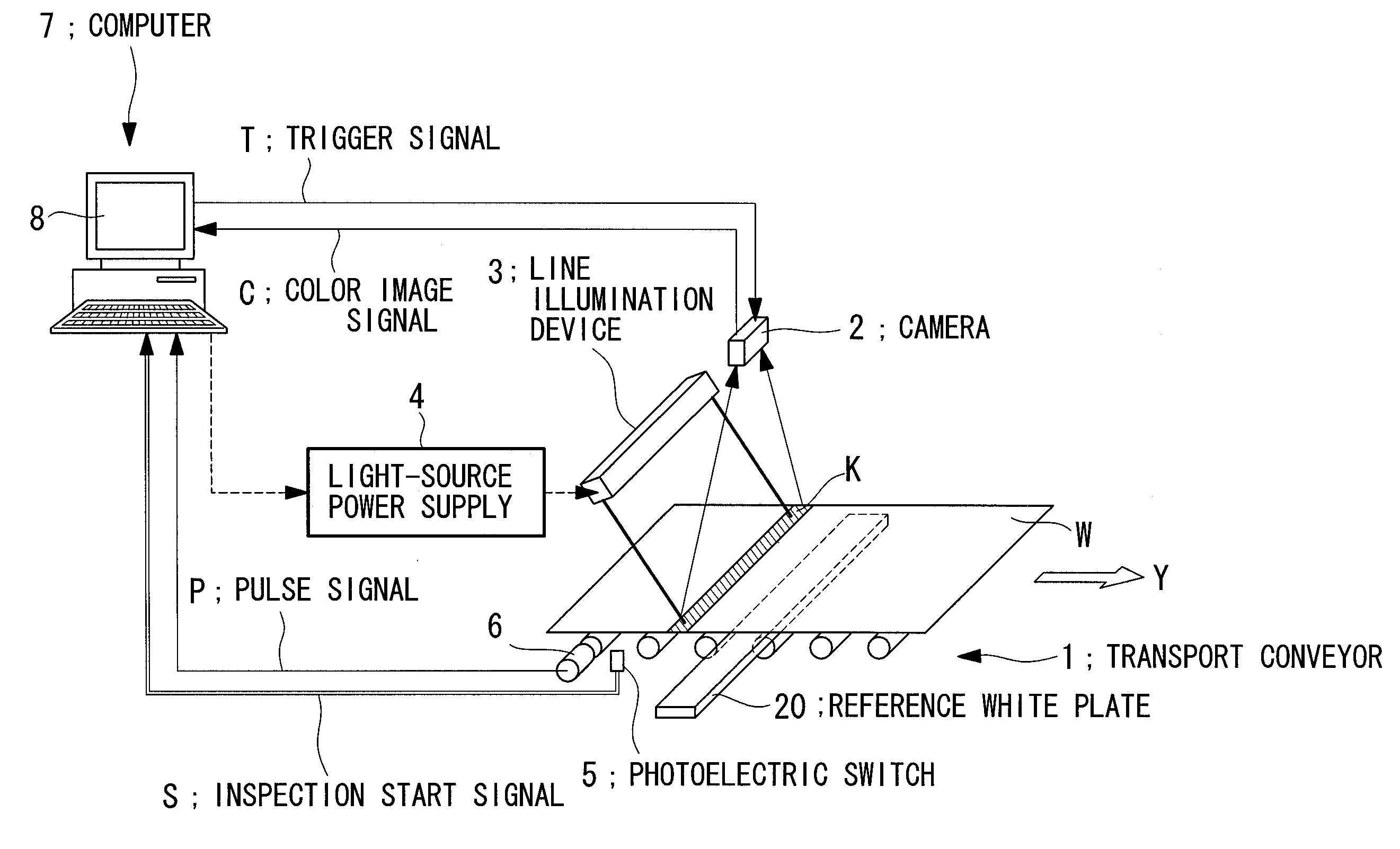
[0050]FIG. 1 is a diagram showing the overall configuration of a film-thickness measurement apparatus according to a first embodiment of the present invention.

[0051]In the film-thickness measurement apparatus shown in FIG. 1, a substrate W is conveyed in a transport direction (Y direction in the figure) by a transport conveyor 1. This substrate W has a transparent electrode film formed by a thermal CVD apparatus, a top cell which is an amorphous silicon film photoelectric conversion layer formed by a plasma CVD apparatus, and an intermediate contact layer formed by a sputtering apparatus, formed in this order on a transparent glass substrate.

[0052]The intermediate contact layer is formed, for example, by laminating 10 nm to 150 nm of GZO (Ga-doped ZnO) with a sputtering apparatus. In FIG. 1, the transport conveyor 1 side of the substrate W is the transparent glass substrate, and the transparent conductive film and the photoelectric conversion layer formed of thin-film silicon are la...

second embodiment

[0086]A film-thickness measurement apparatus according to a second embodiment of the present invention will be described next. The film-thickness measurement apparatus according to this embodiment is substantially the same as the film-thickness measurement apparatus according to the first embodiment described above, but the placement of the camera 2 and the line illumination device 3 is different.

[0087]Differences from the film-thickness measurement apparatus according to the first embodiment will mainly be described below.

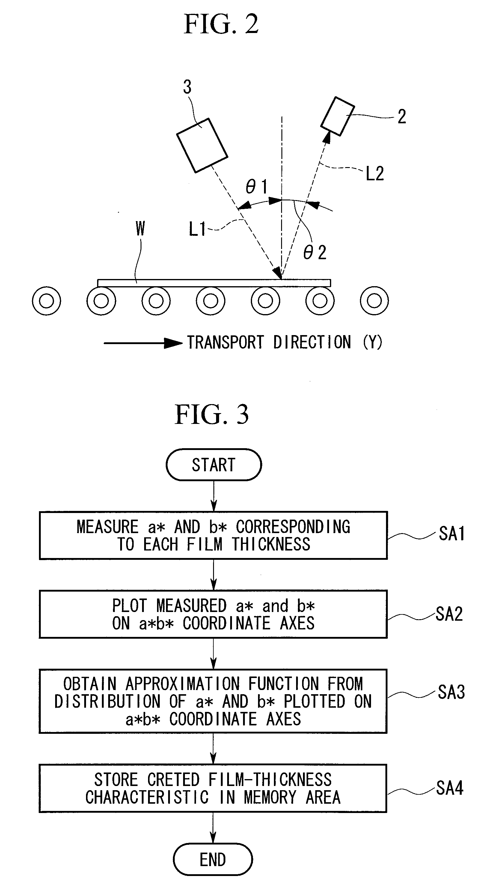
[0088]In the film-thickness measurement apparatus according to this embodiment, the positions at which the camera 2 and the line illumination device 3 are disposed are set so that, in FIG. 2 for example, the incidence angle θ1 of the line illumination light L1 falling on the substrate W is close to about 0°, and the reflection angle θ2 of the line reflected light L2 reflected at the substrate W is any angle from about 0° to about 90°. For example, the positions at...

third embodiment

[0090]Next, a film-thickness measurement apparatus according to a third embodiment of the present invention will be described below. The film-thickness measurement apparatus according to this embodiment is substantially the same as the film-thickness measurement apparatus according to the first embodiment described above, but the placement of the camera 2 and the line illumination device 3 is different.

[0091]Differences from the film-thickness measurement apparatus according to the first embodiment will mainly be described below.

[0092]In the film-thickness measurement apparatus according to this embodiment, the positions at which the camera 2 and the line illumination device 3 are disposed are set so that, in FIG. 2 for example, the incidence angle θ1 of the line illumination light L1 falling on the substrate W and the reflection angle θ2 of the line reflected light L2 reflected at the substrate W are substantially the same. For example, the incidence angle θ1 of the line illuminati...


PUM


Abstract

Objects are to reduce the burden on an operator and to improve fabrication efficiency. A transparent conductive film or a transparent optical film formed on a substrate W is irradiated with line illumination light by means of a line illumination device 3, line reflected light reflected at the transparent conductive film or the transparent optical film is detected with a camera, a color evaluation value of the detected reflected light is measured, and a film thickness corresponding to the measured color evaluation value is obtained using a film-thickness characteristic in which the color evaluation value is associated with the film thickness.

Description

TECHNICAL FIELD[0001]The present invention relates to film-thickness measurement of thin films, and more particularly, to a film-thickness measurement method and apparatus therefor that perform film-thickness measurement of transparent conductive films and transparent optical films used in thin-film devices, as well as to a thin-film device fabrication system.BACKGROUND ART[0002]Thin-film devices include, for example, thin-film solar cells, liquid crystal panels, semiconductor devices, and so on. For example, in the field of thin-film solar cells, except for photoelectric-conversion electricity generating layers (semiconductor material such as silicon) that generate electrical current upon absorption of light, transparent conductive films and transparent optical films that form collector electrodes at the light incident side are used.[0003]Here, taking the example of a tandem solar cell, the balance of the generated currents in a top cell and a bottom cell is corrected by forming a ...

Claims


Application Information

Patent Timeline
Patent Type & Authority Applications(United States)
IPC IPC(8): G01B11/06
CPCG01B11/06Y02E10/50H01L31/206G01B11/0625Y02P70/50
Inventor SAKAI, SATOSHITSUMURA, YOICHIROIIDA, MASAMIKAWAZOE, KOHEI
Owner MITSUBISHI HEAVY IND LTD
Why Eureka
Try Eureka