Printed circuit board

a printed circuit board and circuit board technology, applied in the field of printed circuit boards, can solve the problems of driver inability to implement perfect drive performance, current flowing in the driver is reduced, voltage fluctuation, etc., and achieve the effect of simplifying the power trace and reducing the noise of simultaneous switching

Inactive Publication Date: 2010-07-22
SAMSUNG ELECTRONICS CO LTD
View PDF6 Cites 22 Cited by
  • Summary
  • Abstract
  • Description
  • Claims
  • Application Information

AI Technical Summary

Benefits of technology

[0007]The present general inventive concept provides a printed circuit board (PCB) to reduce simult

Problems solved by technology

In the meantime, current provided from a power layer of the PCB is instantaneously changed when a certain integrated circuit (IC) is switched, such that the current flowing in a ground layer is abruptly changed, resulting in voltage fluctuation.
Due to this SSN, the cu

Method used


Image

  • Printed circuit board
  • Printed circuit board
  • Printed circuit board

Examples


Embodiment Construction

[0033]Reference will now be made in detail to exemplary embodiments of the present general inventive concept, examples of which are illustrated in the accompanying drawings, wherein like reference numerals refer to like elements throughout. The exemplary embodiments are described below in order to explain the present general inventive concept by referring to the figures.

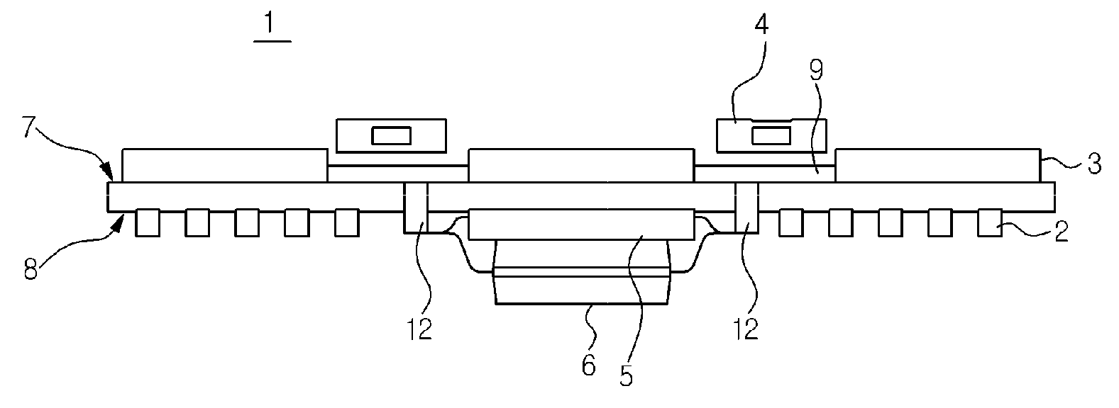
[0034]FIG. 1 is a schematic diagram of a printed circuit board (PCB) 1 according to an exemplary embodiment of the present general inventive concept.

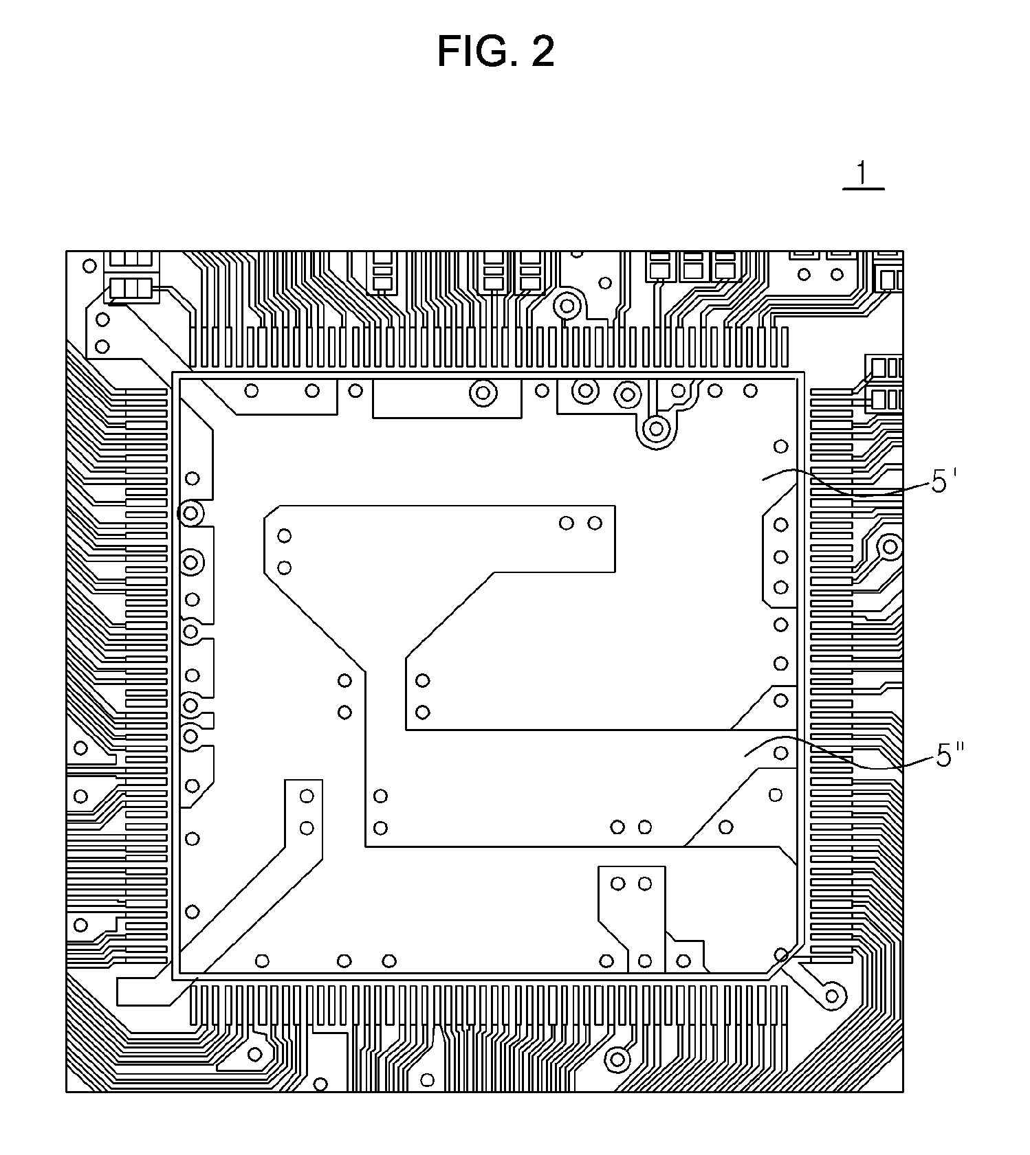
[0035]Referring to FIG. 1, the printed circuit board (PCB) 1 includes a signal trace 2, a ground plane 3, a decoupling capacitor 4, a power plane 5, and a component 6.

[0036]The PCB 1 can be a double-layered printed circuit board in which a first substrate 7 is arranged parallel to a second substrate 8 while being spaced apart from the second substrate 8 by a predetermined distance D. The ground plane 3 can be deposited over the entirety of the first substrate 7. The grou...


PUM


Abstract

A printed circuit board (PCB) reduces a simultaneous switching noise (SSN) causing power noise, thereby reducing radiated electromagnetic interference (EMI). In a double-layered PCB, a first substrate is arranged in parallel with a second substrate while being spaced apart from the second substrate by a predetermined distance. The first substrate includes a ground plane, which is deposited over an entirety of the first substrate. The second substrate includes a power plane deposited at a position of a component mounted to the printed circuit board (PCB) to transmit power to the component. Thus, the power trace of the PCB is simplified in structure, thereby reducing EMI radiation noise.

Description

CROSS-REFERENCE TO RELATED APPLICATIONS[0001]This application claims priority under 35 U.S.C. §119(a) from Korean Patent Application No. 2008-0003843, filed on Jan. 16, 2009 in the Korean Intellectual Property Office, the disclosure of which is incorporated herein by reference in its entirety.BACKGROUND[0002]1. Field of the Invention[0003]The present general inventive concept relates to a printed circuit board for reducing radiated electromagnetic interference (EMI).[0004]2. Description of the Related Art[0005]Generally, a driver and a receiver may be mounted to a printed circuit board (PCB). For example, the driver and the receiver may be a memory controller and a memory each implemented in the form of a chip, respectively. A trace for transmitting a data bus signal is arranged between the driver and the receiver on the PCB. The trace is printed as a conductive medium on the PCB. The data bus signal generated from the driver is switched with a predetermined clock rate, and the swit...

Claims


Application Information

Patent Timeline
IPC IPC(8): H05K1/16H05K1/11
CPCH05K1/0216H05K1/0231H05K2201/093H05K2201/10689H05K2201/09772H05K2201/10522H05K2201/10545H05K2201/09336H05K1/14
Inventor HAN, JANG SOONLEE, SEUNG MYEN
Owner SAMSUNG ELECTRONICS CO LTD
Why Eureka
Try Eureka