Touch panel and electronic device

a technology of electronic devices and touch panels, applied in static indicating devices, instruments, optics, etc., can solve the problems of difficult to maintain mechanical strength, small crystals locally, and disturbance of display, so as to reduce the disturbance of display, improve mechanical strength, and reduce the bend of counter substrates

Inactive Publication Date: 2010-07-22
SEMICON ENERGY LAB CO LTD
View PDF9 Cites 112 Cited by
  • Summary
  • Abstract
  • Description
  • Claims
  • Application Information

AI Technical Summary

Benefits of technology

[0017]According to one embodiment of the present invention, even when an object to be detected is in contact with a touch panel, a constant distance between a pair of substrates which form a touch panel can be kept. Therefore, disturbance of display can be reduced. In addition, even when a TFT substrate is held in a chassis, a bend of a counter substrate can be reduced and the mechanical strength can be improved.

Problems solved by technology

For example, in the case of a touch panel using a liquid crystal panel, when the physical force acts in a direction perpendicular to a substrate of the touch panel, the space between a pair of substrates (a TFT substrate and a counter substrate) which seal a liquid crystal becomes small locally, and display is disturbed.
In that case, however, a counter substrate is bent, and it becomes difficult to maintain the mechanical strength.

Method used


Image

  • Touch panel and electronic device
  • Touch panel and electronic device
  • Touch panel and electronic device

Examples


embodiment 1

[0027]In this embodiment, a touch panel will be described with reference to FIGS. 1 to 4.

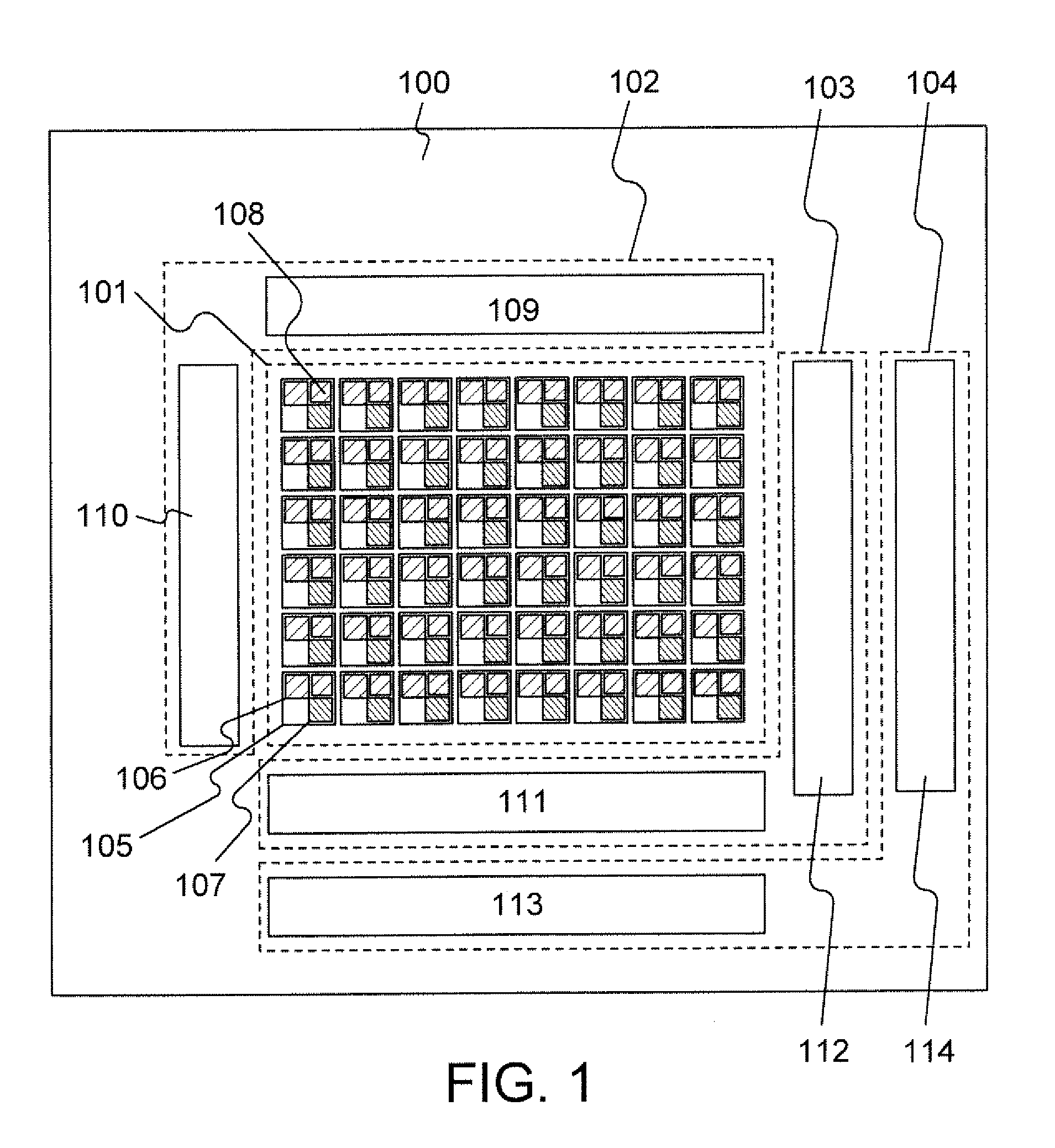
[0028]First, a structure of a touch panel 100 is described with reference to FIG. 1. The touch panel 100 includes a pixel portion 101, a display element control circuit 102, a photosensor control circuit 103, and a MEMS control circuit 104.

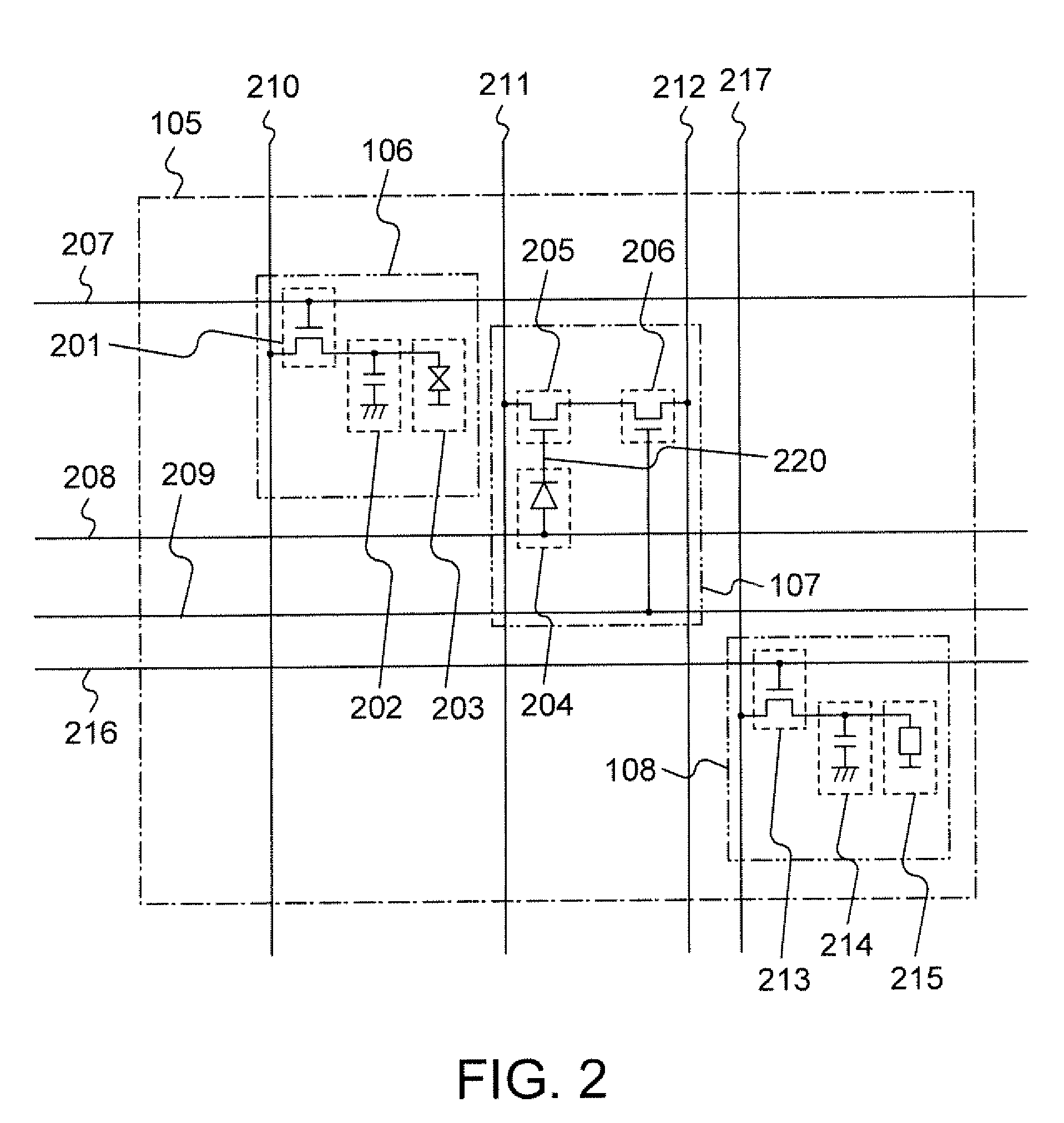
[0029]The pixel portion 101 includes a plurality of pixels 105 arranged in matrix in a row direction and a columnar direction. Each pixel 105 includes a display element portion 106, a photosensor portion 107, and a MEMS portion 108.

[0030]The display element portion 106 includes a thin film transistor (TFT), a storage capacitor, a liquid crystal element in which a liquid crystal layer is sandwiched between a pixel electrode and a counter electrode, a color filter, and the like. In the touch panel 100, since a polarization direction varies when voltage is applied to the liquid crystal layer, the tone (gradation) of light which penetrates the liquid crystal layer...

embodiment 2

[0055]In this embodiment, a touch panel will be described with reference to FIGS. 5A and 5B.

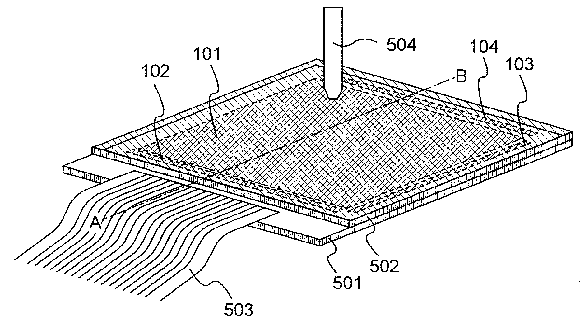
[0056]A touch panel includes a substrate 501 having an insulating surface, the pixel portion 101, the display element control circuit 102, the photosensor control circuit 103, the MEMS control circuit 104, a connection film 503, and a counter substrate 502 (see FIG. 5A). The connection film 503 is connected to an external IC chip.

[0057]A cross-sectional structure taken along line A-B of the touch panel is described with reference to FIG. 5B. The transistor 201 and the liquid crystal element 203 which are included in the display element portion 106, the photodiode 204 included in the photosensor portion 107, and the MEMS element 215 included in the MEMS portion 108 are illustrated. The liquid crystal element 203 includes a pixel electrode 531, a liquid crystal layer 532, and a counter electrode 533. The MEMS element 215 includes an electrode 521, a hollow region 522, and an electrode 523. Over...

embodiment 3

[0065]An example of a cross-sectional structure of a touch panel will be described with reference to FIGS. 6 and 7. First, an example of a cross section of a touch panel using a liquid crystal element as a display element is described with reference to FIG. 6.

[0066]As a substrate 800, a light-transmitting substrate such as a glass substrate or a quartz substrate is used. A thin film transistor 801, a thin film transistor 802, a photosensor 803, and a MEMS element 830 are provided over the substrate 800. The photosensor 803 is formed in such a manner that an n-type semiconductor layer 810, an i-type semiconductor layer 811, and a p-type semiconductor layer 812 are stacked in this order. The n-type semiconductor layer 810 contains an impurity element imparting one conductivity type (e.g., phosphorus). The i-type semiconductor layer 811 is an intrinsic semiconductor. The p-type semiconductor layer 812 contains an impurity element imparting one conductivity type (e.g., boron).

[0067]The ...


PUM


Abstract

To provide a touch panel with reduced disturbance of display and with improved mechanical strength by suppressing variation in the space between a pair of substrates which form the touch panel even when in contact with an object to be detected. A pixel portion including a plurality of pixels is provided between a pair of substrates. Each pixel includes a photosensor portion which detects that the object to be detected is in contact with one of the pair of substrates, and a MEMS portion which generates a mechanical displacement in a direction perpendicular to the pair of substrates when a signal based on a detection result of the photosensor portion is input.

Description

BACKGROUND OF THE INVENTION[0001]1. Field of the Invention[0002]The present invention relates to a touch panel having a touch sensor. In addition, the present invention relates to an electronic device provided with the touch panel.[0003]2. Description of the Related Art[0004]In recent years, a display device provided with a touch sensor has attracted attention. The display device provided with a touch sensor is called a touch panel, a touch screen, and the like (hereinafter simply referred to as a “touch panel”). Examples of the touch sensor include a resistive touch sensor, a capacitance touch sensor, and an optical touch sensor, which are different from each other in operation principle. In any of the sensors, an object to be detected is in contact with a display device or in the vicinity of the display device, whereby data can be input.[0005]By provision of a sensor (also referred to as a “photosensor”) that detects light as an optical touch sensor for a touch panel, a display sc...

Claims


Application Information

Patent Timeline
Patent Type & Authority Applications(United States)
IPC IPC(8): G06F3/042
CPCG02F1/13338G02F2201/44G06F3/0412G06F3/0416G06F3/042G06F3/0421B81B3/0021B81B2201/0264H01L27/1225H01L27/1446G09G3/3648G06F3/04166
Inventor KUROKAWA, YOSHIYUKIIZUMI, KONAMI
Owner SEMICON ENERGY LAB CO LTD
Why Eureka
Try Eureka