System and Method for Improved Automated Semiconductor Wafer Manufacturing

a technology of automated semiconductor wafer manufacturing and manufacturing method, applied in the field of system and method for improving automated semiconductor wafer manufacturing, can solve the problems of increasing inefficiency, affecting the quality of semiconductor wafers, so as to improve the manufacturing process of automated semiconductor wafers

Active Publication Date: 2010-07-22
TAIWAN SEMICON MFG CO LTD
View PDF3 Cites 10 Cited by
  • Summary
  • Abstract
  • Description
  • Claims
  • Application Information

AI Technical Summary

Problems solved by technology

Generally, some level of misalignment occurs between the layers during the production process.
One of the most difficult areas to correct overlay misalignment involves leading lots, the initial group of wafers produced with a mask and tool combination.
Human involvement and frequent mask changes that require alignment increase inefficiency and greatly increase semiconductor production time.
Additionally, these automated systems cause process interlock that increases operation loading because the operator cannot visually identify the leading lot wafers.
Failure to record overlay alignment values introduces additional rework due to misalignment because the system cannot relate and adjust the present production process based on the experiences of past production processes.

Method used


Image

  • System and Method for Improved Automated Semiconductor Wafer Manufacturing
  • System and Method for Improved Automated Semiconductor Wafer Manufacturing
  • System and Method for Improved Automated Semiconductor Wafer Manufacturing

Examples


Embodiment Construction

[0017]The making and using of the presently preferred embodiments are discussed in detail below. It should be appreciated, however, that the present invention provides many applicable inventive concepts that can be embodied in a wide variety of specific contexts. The specific embodiments discussed are merely illustrative of specific ways to make and use the invention, and do not limit the scope of the invention.

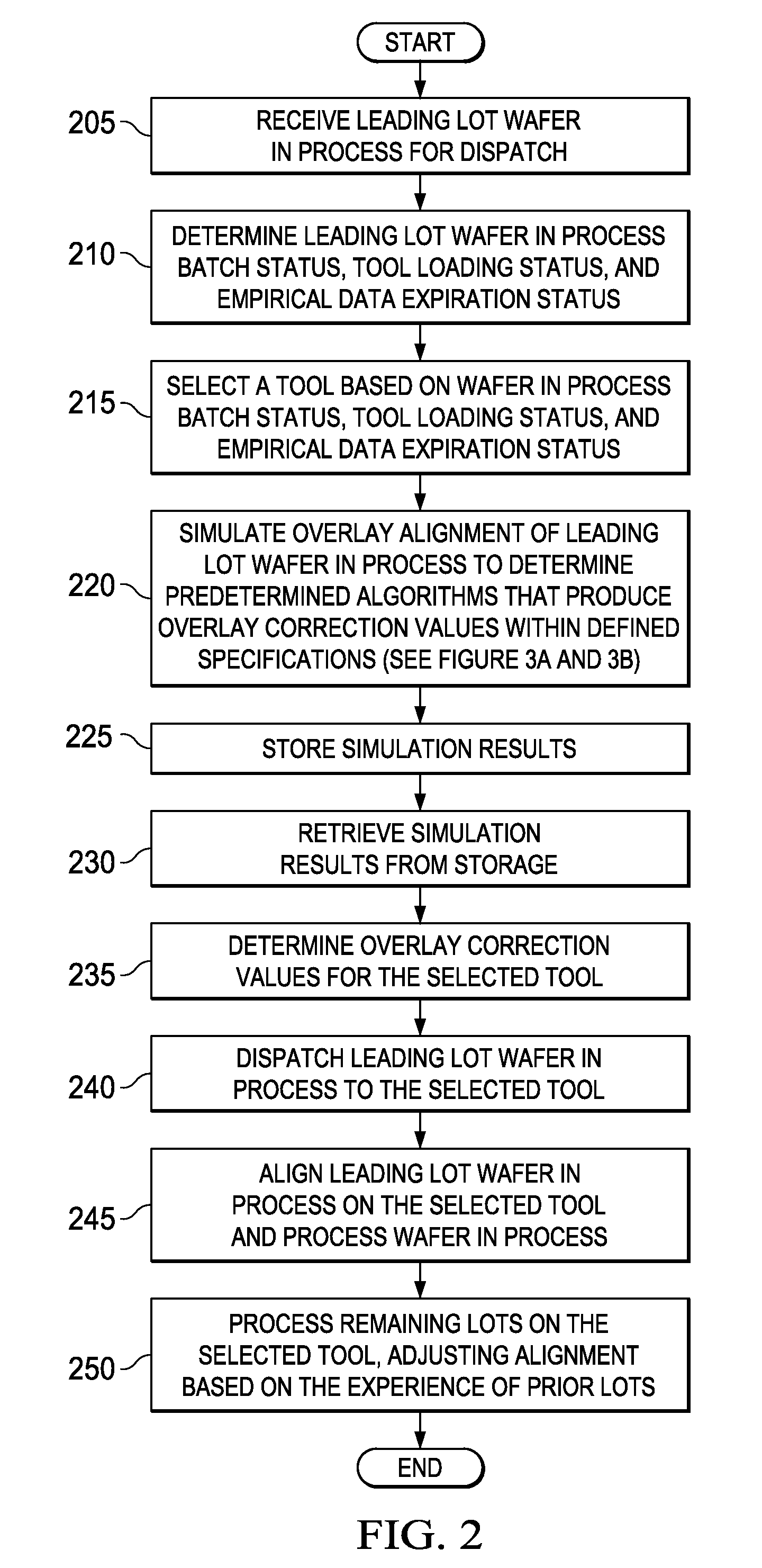
[0018]The present invention will be described with respect to preferred embodiments in a specific context, namely a system for processing leading lot wafers on a selected tool based on an improved algorithm simulation.

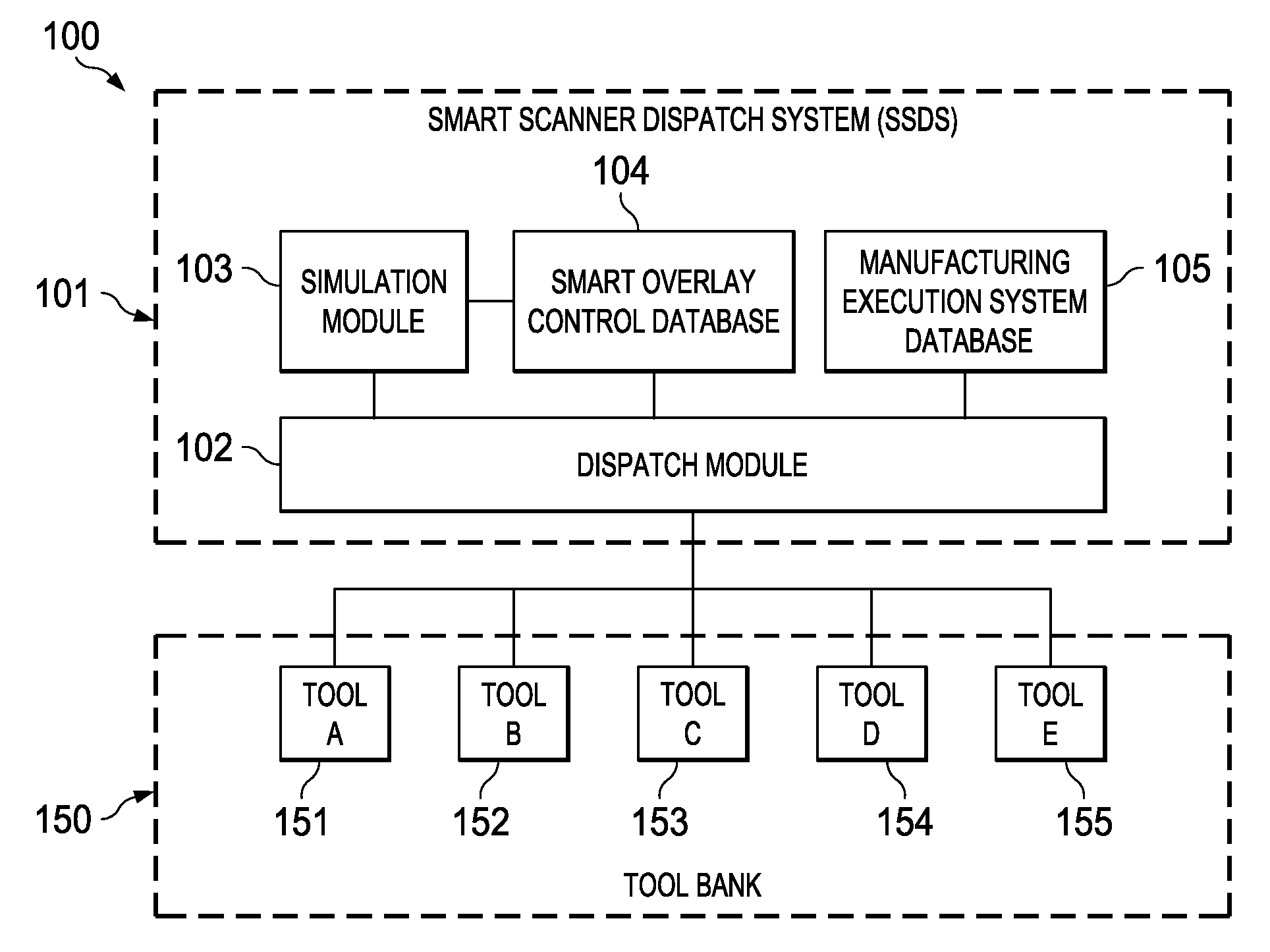
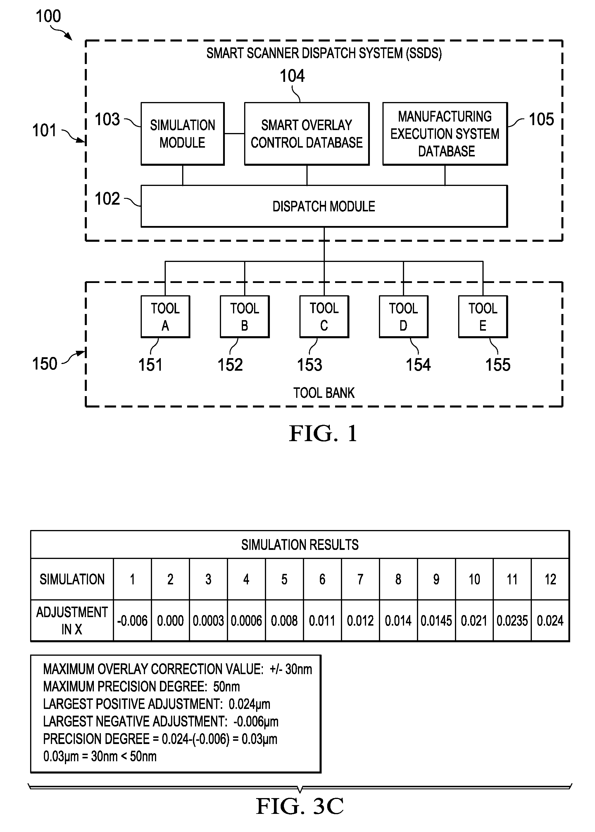
[0019]With reference now to FIG. 1, there is shown a schematic diagram illustrating elements of a system 100 for wafer dispatch. Specifically, system 100 comprises a smart scanner dispatch system (SSDS) 101 and a tool bank 150. The tool bank 150 preferably comprises a plurality of tools represented by Tool A 151, Tool B 152, Tool C 153, Tool D 154, and Tool E 15...


PUM


Abstract

System and method for automated semiconductor manufacturing is provided. In accordance with one aspect of the present invention, a system for automated semiconductor wafer manufacturing includes a smart overlay control (SOC) database having empirical alignment data related to overlay alignment, and a simulation module communicatively coupled to the SOC database, the simulation module determining a simulated overlay alignment of a wafer on the plurality of photolithography tools in a tool bank based on the empirical alignment data stored in the SOC database. The system also includes a dispatch module communicatively coupled to the SOC database and the simulation module, the dispatch module controlling the dispatch of a wafer to one of a plurality of photolithography tools in a tool bank based at least in part on the simulated overlay alignment.

Description

[0001]This application claims the benefit of U.S. Provisional Application No. 61 / 146,582, filed on Jan. 22, 2009, entitled “System and Method for Improved Automated Semiconductor Wafer Manufacturing,” which application is hereby incorporated herein by reference.TECHNICAL FIELD[0002]The present invention relates generally to a system and method for improved automated semiconductor wafer manufacturing and, more particularly, to a system and method for identifying an algorithm to align leading lots.BACKGROUND[0003]Modern photolithographic semiconductor fabrication processes produce integrated circuits on a semiconductor wafer by forming patterns in successive layers. One method of creating a layer is to form a layer of a desired material, form a photoresist layer on the material layer, expose light through a mask to impinge upon the photoresist, and develop the photoresist to create a pattern. The wafer is then etched, removing selected portions of the material underlying the photoresi...

Claims


Application Information

Patent Timeline
Patent Type & Authority Applications(United States)
IPC IPC(8): G06F17/50G06G7/66
CPCG03F7/70458G05B19/402G05B19/41885G05B2219/45031G05B19/02Y10S438/975Y02P90/26Y02P90/20Y02P90/02
Inventor HSIEH, WEN-YAOCHIU, CHE-YUPENG, ANWEICHEN, JIAN-HUNGWU, HSUCH-CHEN
Owner TAIWAN SEMICON MFG CO LTD
Why Eureka
Try Eureka