Manufacturing method of thin film transistor and manufacturing method of display device

a manufacturing method and technology of thin film transistor, applied in the direction of transistors, semiconductor devices, electrical devices, etc., can solve the problems of reducing reducing the yield, and difficult to further reduce the number of photomasks, so as to improve throughput and reduce leakage current

Active Publication Date: 2010-07-29
SEMICON ENERGY LAB CO LTD
View PDF44 Cites 18 Cited by
  • Summary
  • Abstract
  • Description
  • Claims
  • Application Information

AI Technical Summary

Benefits of technology

[0041]In addition, a step of drying and the like after the second etching is unnecessary, which results in improving throughput.
[0042]Since a thin film transistor manufactured by any of the

Problems solved by technology

Using such complicated techniques may cause various problems, which leads to reduction in yield.
Further, in many cases, reduction in the number of photomasks i

Method used


Image

  • Manufacturing method of thin film transistor and manufacturing method of display device
  • Manufacturing method of thin film transistor and manufacturing method of display device
  • Manufacturing method of thin film transistor and manufacturing method of display device

Examples


embodiment 1

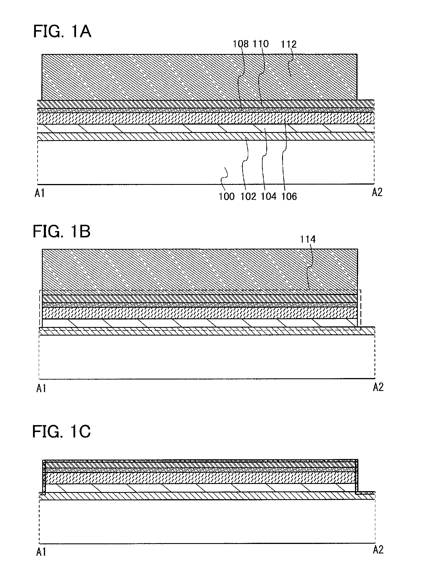
[0103]In this embodiment, an example of a method for manufacturing a thin film transistor and a method for manufacturing a display device in which the thin film transistors are arranged in a matrix form will be described with reference to FIG. 1A to FIG. 29C.

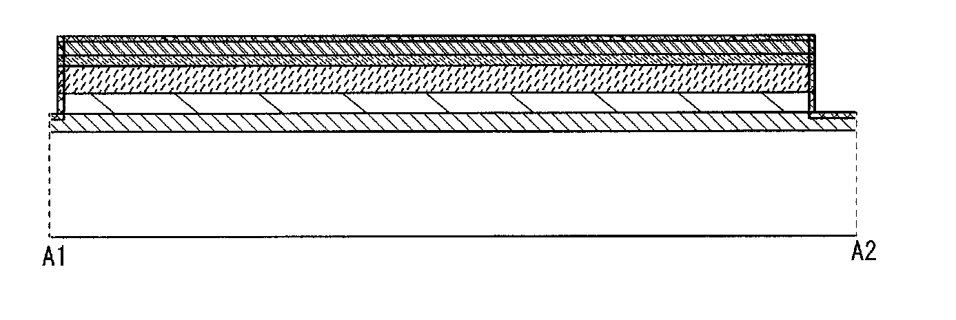
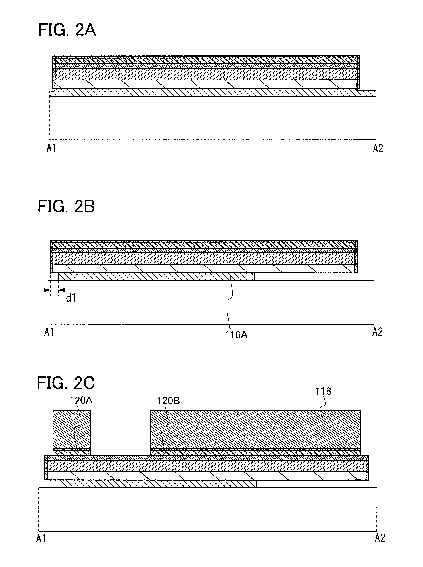
[0104]FIG. 21, FIG. 22, FIG. 23, FIG. 24, and FIG. 25 are top views of thin film transistors of this embodiment. FIG. 25 is a completion drawing in the situation that formation of a pixel electrode is finished. FIGS. 1A to 1C, FIGS. 2A to 2C, FIGS. 3A to 3C, and FIGS. 4A and 4B are cross-sectional views taken along line A1-A2 in FIG. 21, FIG. 22, FIG. 23, FIG. 24, and FIG. 25. FIGS. 5A to 5C, FIGS. 6A to 6C, FIGS. 7A to 7C, and FIGS. 8A and 8B are cross-sectional views taken along line B1-B2 in FIG. 21, FIG. 22, FIG. 23, FIG. 24, and FIG. 25. FIGS. 9A to 9C, FIGS. 10A to 10C, FIGS. 11A to 11C, and FIGS. 12A and 12B are cross-sectional views taken along line C1-C2 in FIG. 21, FIG. 22, FIG. 23, FIG. 24, and FIG. 25. FIGS. 13A to 1...

embodiment 2

[0215]In this embodiment, a method for manufacturing a thin film transistor and a method for manufacturing a display device, which are different from those of Embodiment 1, will be described. Specifically, a method for manufacturing a thin film transistor which is similar to that of Embodiment 1, using a multi-tone mask will be described with reference to FIGS. 31A and 31B, FIGS. 32A to 32C, FIGS. 33A to 33C, FIG. 34, FIG. 35, and FIG. 36.

[0216]FIGS. 32A to 32C correspond to FIGS. 1A to 1C, and FIGS. 2A to 2C of Embodiment 1. FIGS. 33A to 33C correspond to FIGS. 13A to 13C, and FIGS. 14A to 14C of Embodiment 1. FIG. 34, FIG. 35, and FIG. 36 correspond to FIG. 21, FIG. 22, and FIG. 23 of Embodiment 1. The cross-sectional views taken along line A1-A2 illustrated in FIG. 34, FIG. 35, and FIG. 36 correspond to FIGS. 32A to 32C, and the cross-sectional views taken along line D1-D2 illustrated in FIG. 34, FIG. 35, and FIG. 36 correspond to FIGS. 33A to 33C.

[0217]First, as in Embodiment 1,...

embodiment 3

[0245]In this embodiment, a method for manufacturing a thin film transistor and a method for manufacturing a display device according to the present invention, which are different from those of Embodiments 1 and 2, will be described. Specifically, a mode in which a first conductive film 102 is etched by the first etching which is described in Embodiments 1 and 2 will be described with reference to FIGS. 37A to 37C, FIGS. 38A to 38C, FIGS. 39A to 39C, FIGS. 40A to 40C, FIGS. 41A to 41C, and FIG. 42.

[0246]Note that FIGS. 37A to 37C correspond to FIGS. 1A to 1C and FIGS. 2A to 2C of Embodiment 1. FIGS. 38A to 38C correspond to FIGS. 5A to 5C and FIGS. 6A to 6C of Embodiment 1. FIGS. 39A to 39C correspond to FIGS. 9A to 9C and FIGS. 10A to 10C of Embodiment 1. FIGS. 40A to 40C correspond to FIGS. 13A to 13C and FIGS. 14A to 14C of Embodiment 1. FIGS. 41A to 41C correspond to FIGS. 17A to 17C and FIGS. 18A to 18C of Embodiment 1. FIG. 42 corresponds to FIG. 21 of Embodiment 1.

[0247]First...


PUM


Abstract

To provide a method for manufacturing a thin film transistor and a display device using a small number of masks, a thin film transistor is manufactured in such a manner that a first conductive film, an insulating film, a semiconductor film, an impurity semiconductor film, and a second conductive film are stacked; then, a resist mask is formed thereover; first etching is performed to form a thin-film stack body; second etching in which the first conductive film is side-etched is performed by dry-etching to form a gate electrode layer; and a source electrode, a drain electrode, and the like are formed. Before the dry etching, it is preferred that at least a side surface of the etched semiconductor film be oxidized.

Description

BACKGROUND OF THE INVENTION[0001]1. Field of the Invention[0002]The present invention relates to manufacturing methods of a thin film transistor and a display device including the thin film transistor.[0003]2. Description of the Related Art[0004]In recent years, thin film transistors that are formed using a semiconductor thin film having a thickness of several nanometers to several hundreds of nanometers over a substrate having an insulating surface such as a glass substrate have been attracting attentions. Thin film transistors are widely used for electronic devices such as ICs (integrated circuits) and electro-optical devices. In particular, thin film transistors are urgently developed as switching elements of display devices typified by liquid crystal display devices, electro luminescence (EL) display devices, and the like. In active matrix liquid crystal display devices, specifically, voltage is applied between a pixel electrode connected to a selected switching element and a co...

Claims


Application Information

Patent Timeline
IPC IPC(8): H01L29/786H01L21/336
CPCH01L27/1288H01L27/1214
Inventor SUZAWA, HIDEOMIMIZOGUCHI, TAKAFUMIDAIRIKI, KOJIMIKAMI, MAYUMISAITO, YUMIKO
Owner SEMICON ENERGY LAB CO LTD
Why Eureka
Try Eureka