Suspended mono-crystalline structure and method of fabrication from a heteroepitaxial layer

Inactive Publication Date: 2010-07-29
HEWLETT PACKARD DEV CO LP
View PDF15 Cites 4 Cited by
  • Summary
  • Abstract
  • Description
  • Claims
  • Application Information

AI Technical Summary

Problems solved by technology

In particular, many devices including, but not limited to, devices fabricated from certain compound semiconductors (e.g., III-V and II-VI compound semiconductors), would not be practical without epitaxial deposition.
Unfortunately, heteroepitaxial deposition often produces mono-crystalline layers of material that are less than ideal for use in realizing high-performance devices.
In particular, a mismatch between a lattice constant of the crystalline substrate and the heteroepitaxial layer deposited on the substrate often exists.
Such a ‘lattice mismatch’ introduces elastic strain in the heteroepitaxial layer that ultimately results in the formation of misfit and threading dislocations or simply ‘lattice defects’ in the heteroepitaxial layer.
These lattice defects adversely affect the electrical properties of the heteroepitaxial layer, in part, by trapping charges at dangling bonds, thereby degrading current flow within the heteroepitaxial layer.
Further, the lattice defects are often associated with or produce unacceptably high leakage currents in an OFF state of a device (e.g., diode junctions) fabricated in the heteroepitaxial layer.
Such lattice defects due to the lattice mismatch between the heteroepitaxial layer and the underlying substrate have often frustrated the adoption of a wide variety of otherwise attractive material combinations for various electronic, photonic and mixed use applications.
However, even the relatively lower permittivity of solid-state material layers such as an oxide (e.g., SiO2) may still limit high-performance devices.
Although a suspended polycrystalline semiconductor layer may be adequate for some applications, it is not suitable for many high-performance devices.
Such high-performance devices generally require a single-crystal layer which cannot be provided using a sacrificial oxide.

Method used


Image

  • Suspended mono-crystalline structure and method of fabrication from a heteroepitaxial layer
  • Suspended mono-crystalline structure and method of fabrication from a heteroepitaxial layer
  • Suspended mono-crystalline structure and method of fabrication from a heteroepitaxial layer

Examples


Embodiment Construction

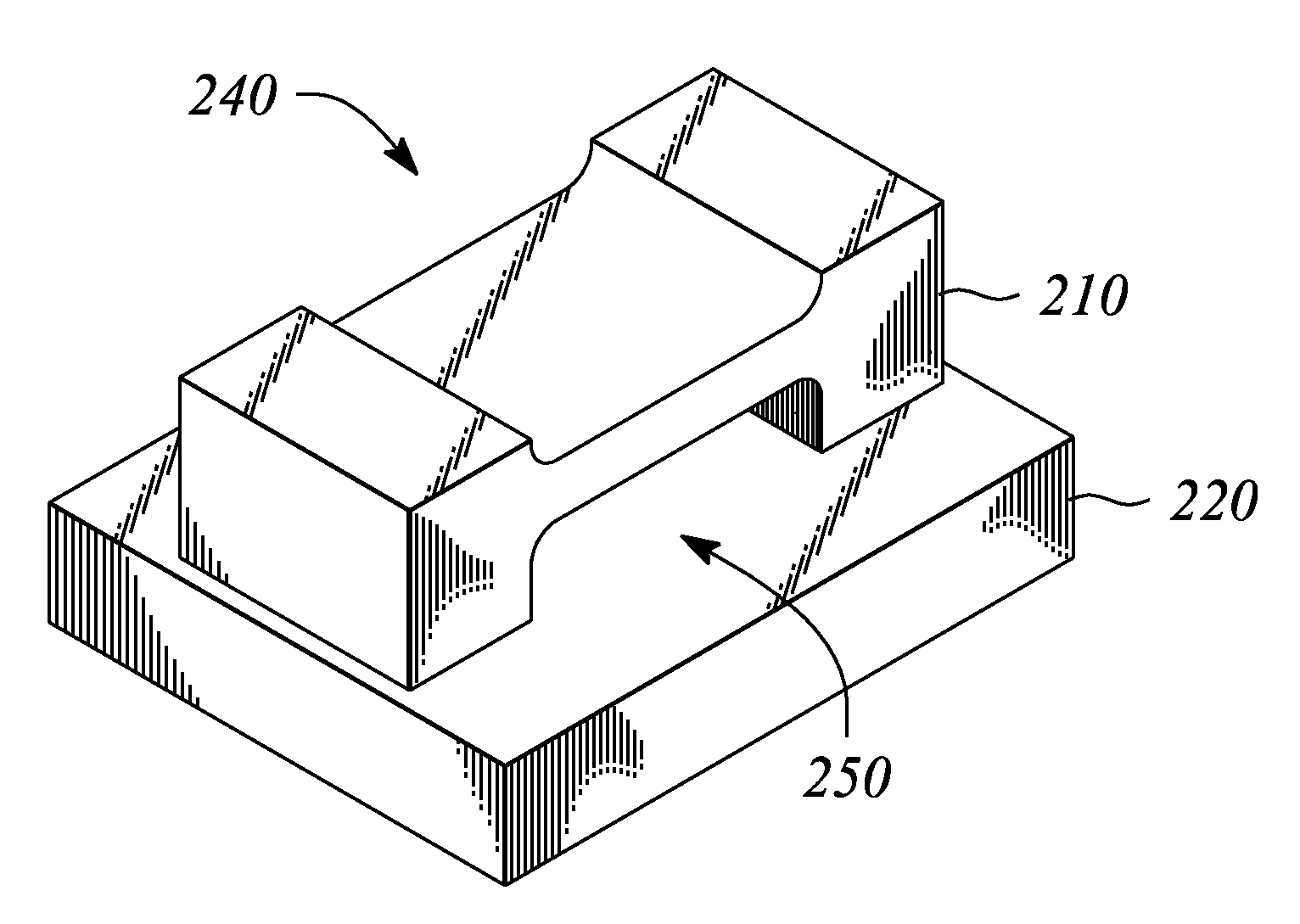
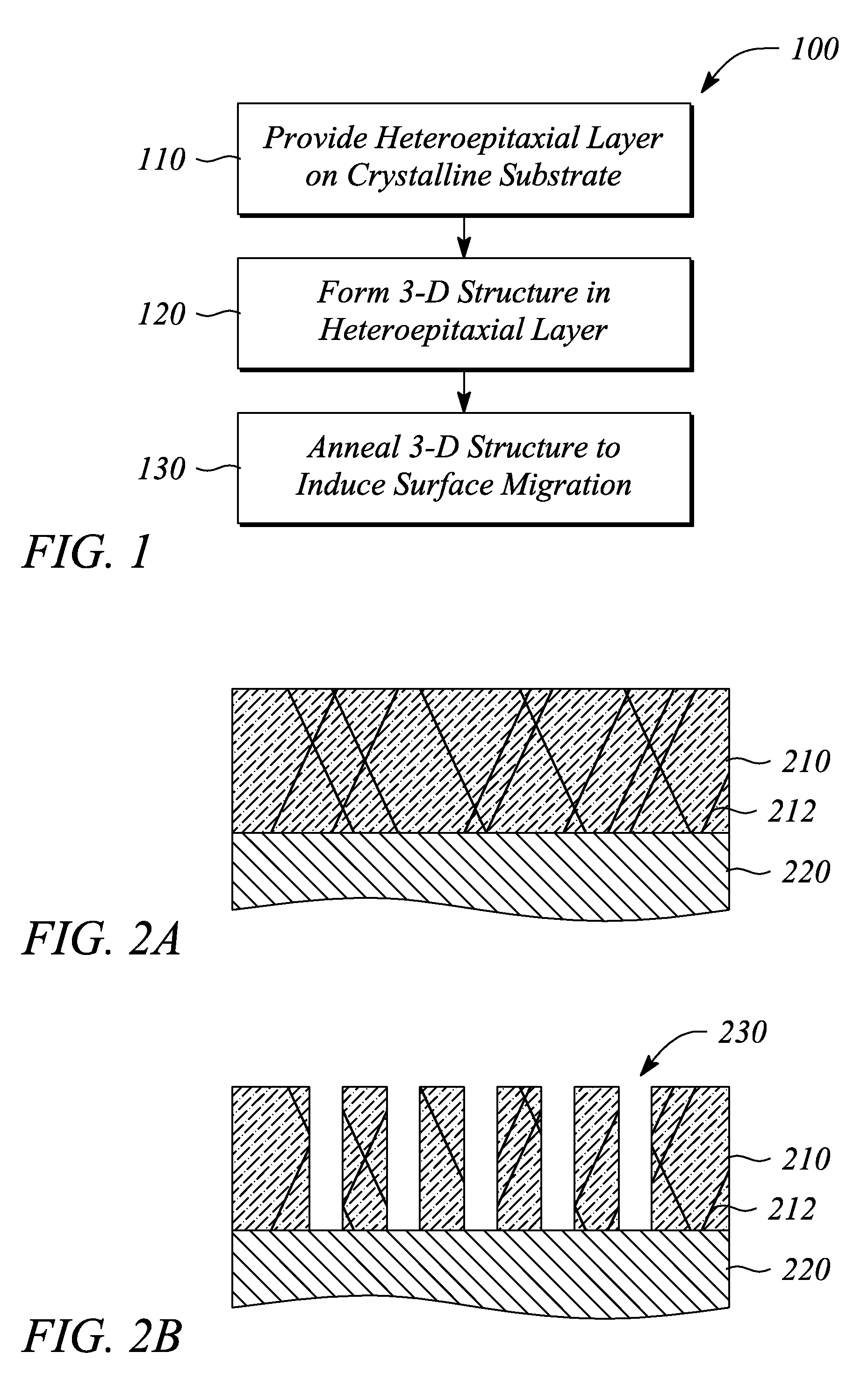
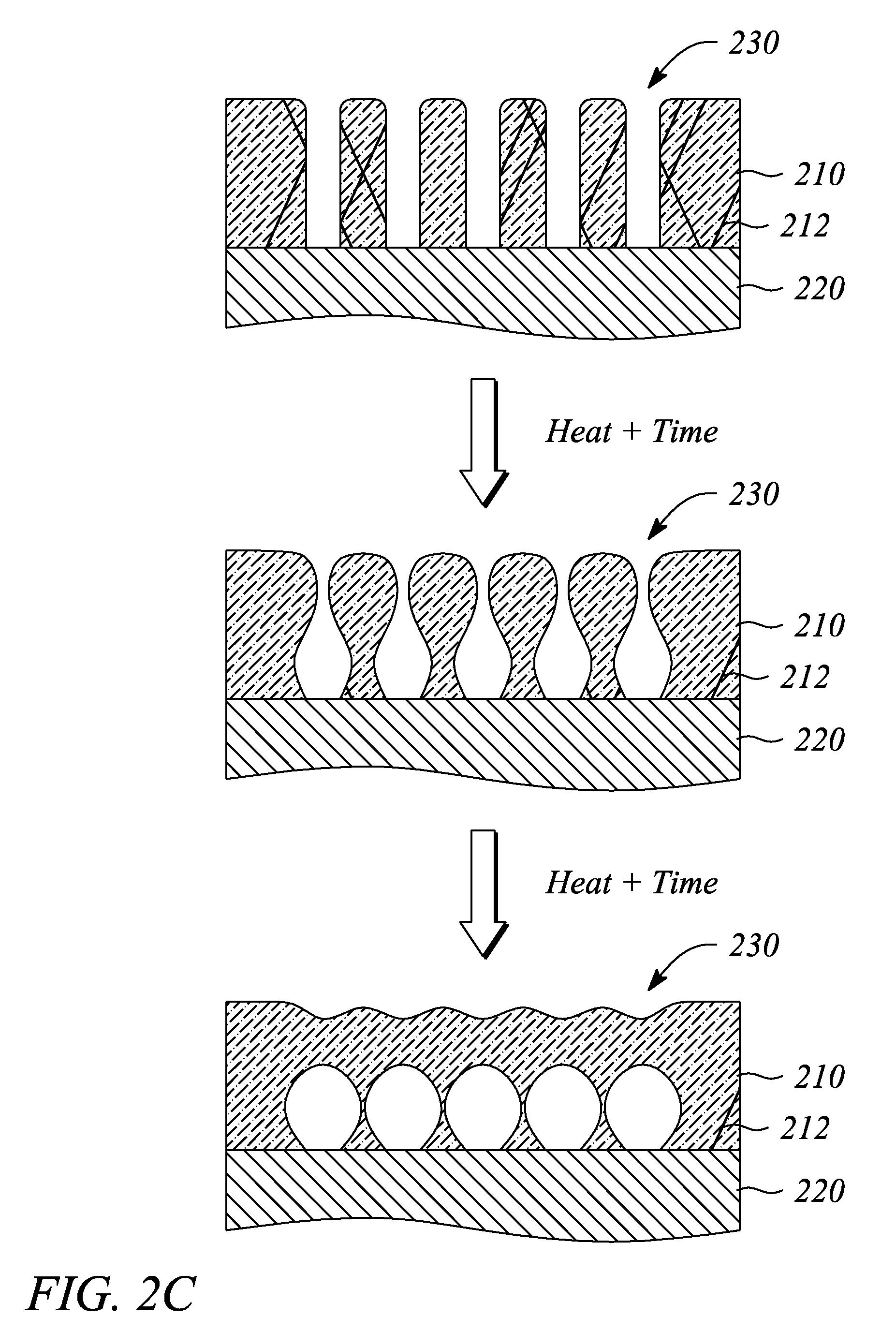
[0029]Embodiments of the present invention facilitate realizing a mono-crystalline structure suspended above an underlying crystalline substrate. For example, embodiments of the present invention may provide a so-called ‘semiconductor-on-nothing’ structure. The suspended mono-crystalline structure comprises a single crystal of a crystalline material and is formed from a heteroepitaxial layer that has an epitaxial connection with the underlying crystalline substrate, according to the present invention. In some embodiments, the suspended mono-crystalline structure may have fewer lattice defects than the heteroepitaxial layer from which the suspended mono-crystalline structure is formed. In particular, a suspended portion of the heteroepitaxial layer that forms the suspended mono-crystalline structure may have a lower lattice defect density than portions of the heteroepitaxial layer that are not suspended, according to some embodiments.

[0030]As noted above, the suspended mono-crystalli...


PUM


Abstract

Methods of fabricating a suspended mono-crystalline structure use annealing to induce surface migration and cause a surface transformation to produce the suspended mono-crystalline structure above a cavity from a heteroepitaxial layer provided on a crystalline substrate. The methods include forming a three dimensional (3-D) structure in the heteroepitaxial layer where the 3-D structure includes high aspect ratio elements. The 3-D structure is annealed at a temperature below a melting point of the heteroepitaxial layer. The suspended mono-crystalline structure may be a portion of a semiconductor-on-nothing (SON) substrate.

Description

CROSS-REFERENCE TO RELATED APPLICATIONS[0001]N / ASTATEMENT REGARDING FEDERALLY SPONSORED RESEARCH OR DEVELOPMENT[0002]N / ABACKGROUND[0003]1. Technical Field[0004]The invention relates to semiconductor fabrication and semiconductor devices. In particular, the invention relates to mono-crystalline structures in semiconductor devices.[0005]2. Description of Related Art[0006]Epitaxy or more generally epitaxial deposition represents a nearly indispensible step in the fabrication of many modern semiconductor devices. Epitaxial deposition may be used to create mono-crystalline layers of high quality crystalline films with ultra-high purity. For example, silicon (Si) epitaxy is often used to provide an ultra-pure layer of Si crystal on an underlying Si wafer. The ultra-pure Si layer is then used as a layer for realizing various devices through additional processing steps. Epitaxy is also a principal means for realizing mono-crystalline layers or films comprising materials and compositions not...

Claims


Application Information

Patent Timeline
IPC IPC(8): H01L29/267H01L21/20
CPCB81C1/00142B81C1/00158B81C2201/0116H01L29/0657H01L21/02521H01L21/02667H01L21/764H01L21/0237
Inventor CHO, HANS S.KAMINS, THEODORE I.
Owner HEWLETT PACKARD DEV CO LP
Why Eureka
Try Eureka