Semiconductor device and method of manufacturing the same

a semiconductor chip and semiconductor technology, applied in the direction of semiconductor devices, semiconductor/solid-state device details, electrical equipment, etc., can solve the problems of reducing the joint strength, affecting the performance of the semiconductor chip, and the ag paste or between the metal leadframe and the ag paste in the semiconductor chip is decreased, so as to prevent the fatigue failure of the metal portion and increase the joint strength and bendability of the bonding portion

Active Publication Date: 2010-07-29
RENESAS ELECTRONICS CORP
View PDF1 Cites 67 Cited by
  • Summary
  • Abstract
  • Description
  • Claims
  • Application Information

AI Technical Summary

Benefits of technology

[0011]There can be provided a Pb-free bonding portion that prevents fatigue failure of a metal portion upon temperature variation in the semiconductor chip by increasing joint strength and bendability of the bonding portion of the semiconductor device and has an equivalent reliability under thermal cycle test to that of a conventional high Pb content solder.

Problems solved by technology

Therefore, there are problems such that joint strength at an interface between the rear-surface electrode and the Ag paste or between the metal leadframe and the Ag paste in the semiconductor chip is decreased by moisture influence at the joint portion of the Ag paste to cause delamination, and that moisture penetrates into the Ag-paste resin and bubbles are formed at an interface between the Ag-paste resin and the molding compounds or inside the molding compounds in a step of molding the molding compounds and heating it to harden.
Also, in the case of die-bonding by the sintering-type metal bond paste, since a die-bonding layer has a fine-porous structure, the plating solution penetrating in the joint layer cannot be completely removed in a cleaning step after the plating step.
Therefore, residual ionic impurities in the joint layer cause problems such as the decrease of reliability of the semiconductor device against high temperature and high humidity and the decrease of productivity because of requirement of time for the cleaning step and a drying step.
Further, in a method of carrying out the plating after filling the porous portion with resin, there is a problem such that moisture of the plating solution penetrates into the resin and bubbles are formed at an interface of the molding compounds or inside the molding compounds in a step of molding the molding compounds and heating it to harden like in the case of the Ag paste.

Method used


Image

  • Semiconductor device and method of manufacturing the same
  • Semiconductor device and method of manufacturing the same
  • Semiconductor device and method of manufacturing the same

Examples


first embodiment

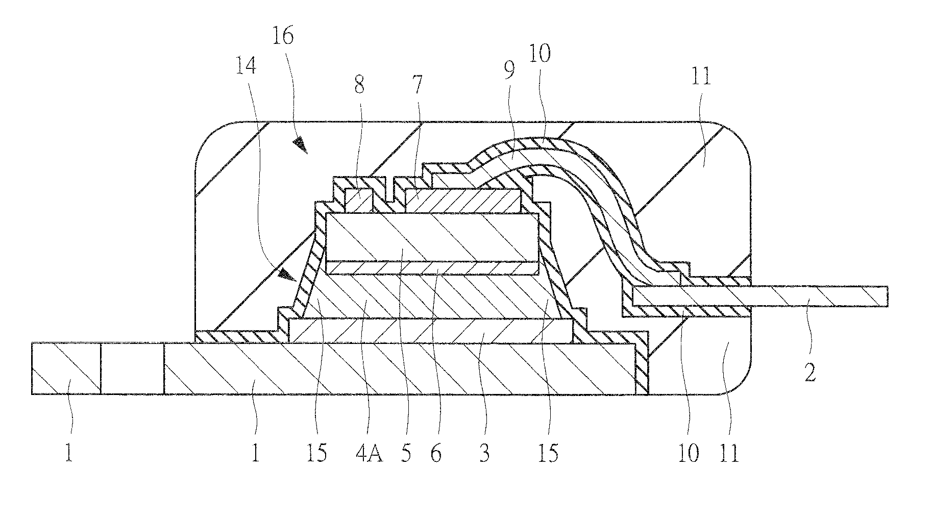
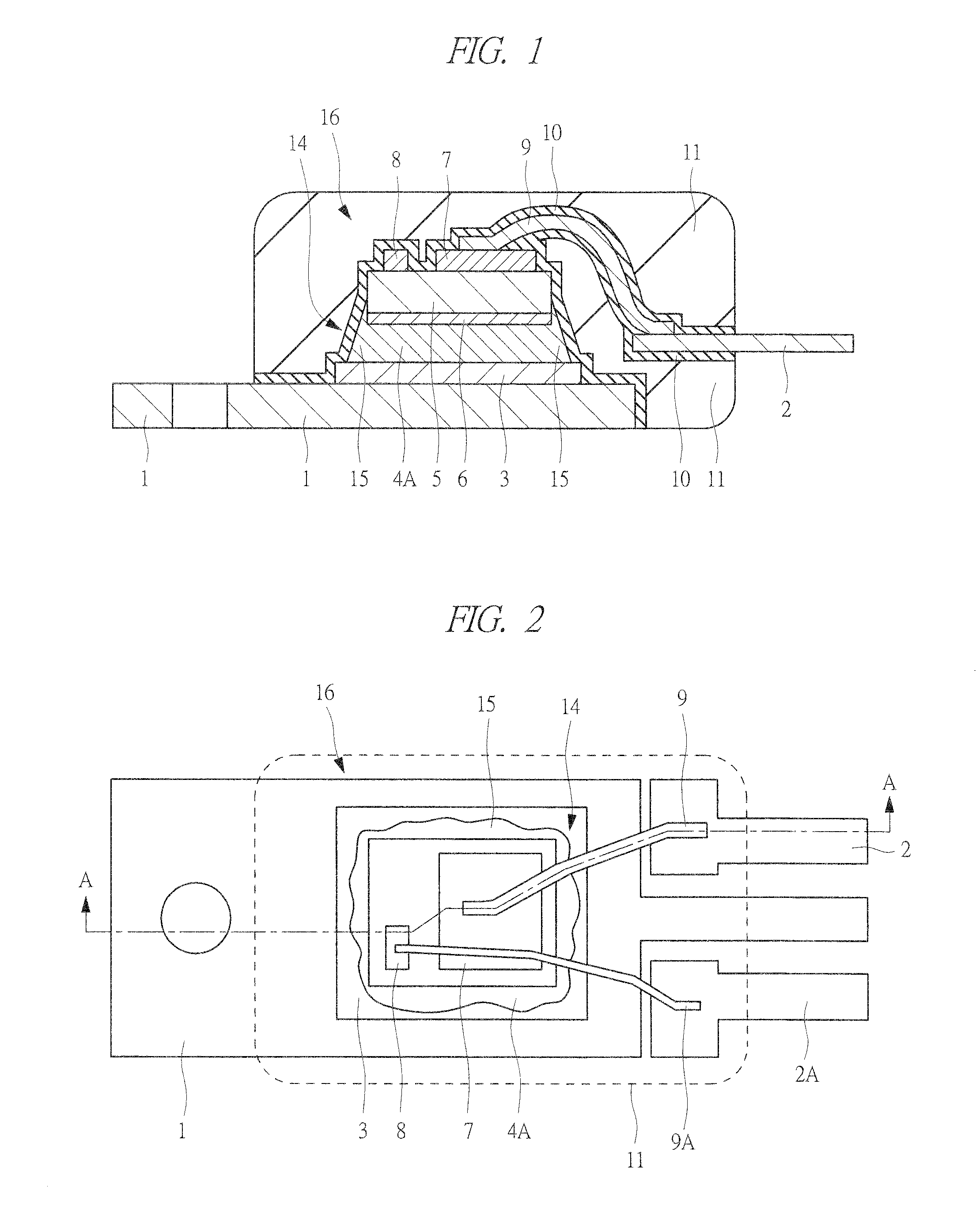
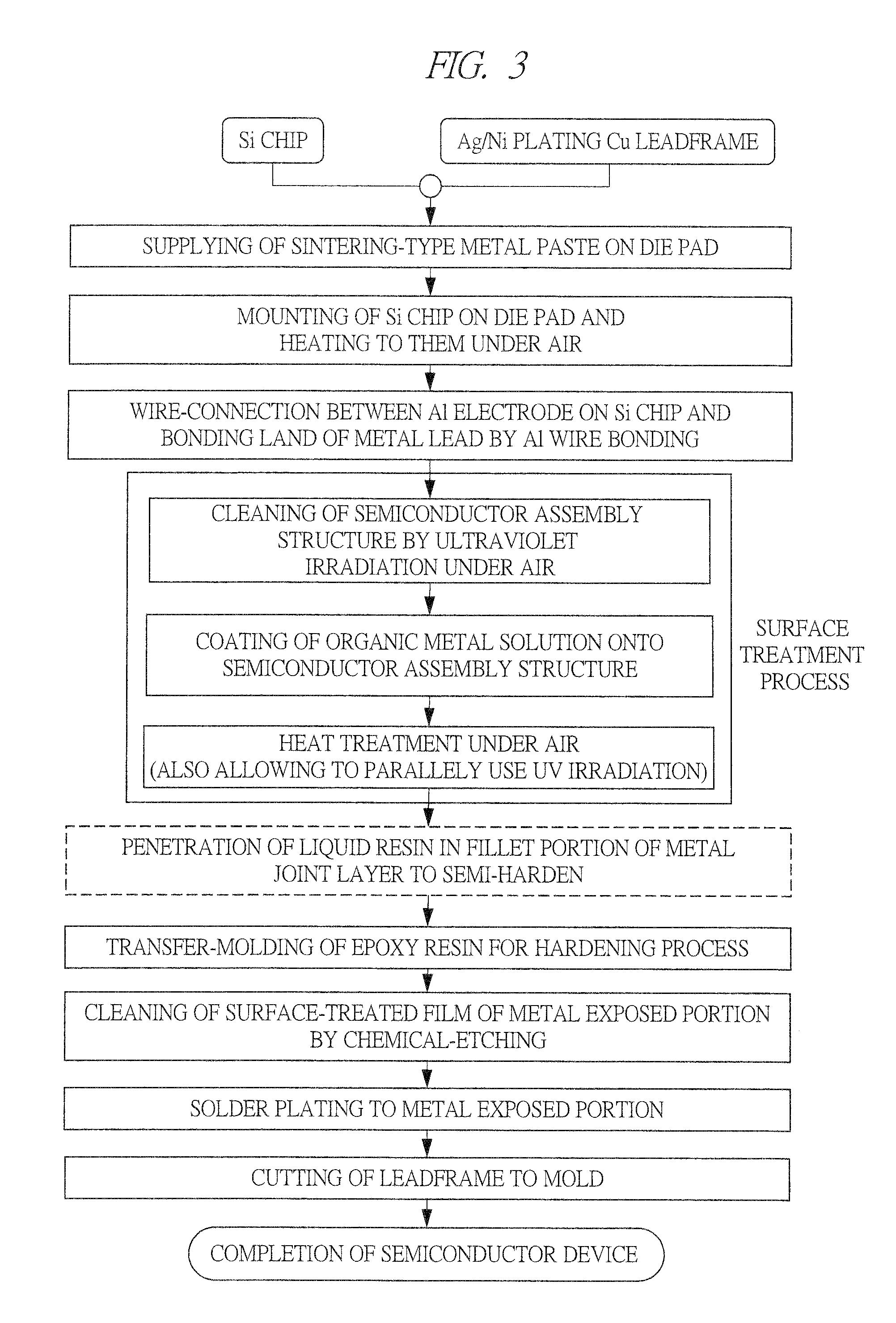
[0033]In the present embodiment, the present invention is applied to a method of manufacturing a semiconductor device, and the first embodiment will be described with reference to FIGS. 1 to 8.

[0034]FIGS. 1 and 2 illustrate a structure of a semiconductor device according to the present embodiment. FIG. 1 illustrates a cross-sectional view taken along a line A-A in FIG. 2. FIG. 2 is a top-surface plan view of the semiconductor device according to the present embodiment. Note that, in FIG. 2, epoxy molding compounds 11 in FIG. 1 are illustrated by a dash line, and a film 10 is not illustrated.

[0035]In FIGS. 1 and 2, a rear-surface electrode 6 made of a metal such as gold is formed on a rear surface of a Si (silicon) chip 5, which is a vertical semiconductor chip having an electrode on its rear surface like an IGBT and a power MOSFET, and a main electrode 7 and a control electrode 8 each formed of an Al (aluminum) film are formed on a main surface of the Si chip 5. An Ag (silver)-plati...

second embodiment

[0058]In the present embodiment, the present invention is applied to a method of manufacturing a semiconductor device, and the second embodiment will be described with reference to FIGS. 10 and 11.

[0059]FIGS. 10 and 11 illustrate a structure of a semiconductor device according to the present embodiment. FIG. 10 illustrates a cross-sectional view taken along a line B-B in FIG. 11. FIG. 11 illustrates a top-surface plan view of the semiconductor device according to the present embodiment. Note that, in FIG. 11, epoxy molding compounds 28 in FIG. 10 are illustrated by a dotted line, and a film 26 and an Ag-plating film 30 are not illustrated.

[0060]In FIGS. 10 and 11, a rear-surface electrode 20 made of a metal such as gold is formed on a rear surface of a Si chip 19 which is a vertical semiconductor chip, and a main electrode 22 in which Ni / Au is formed on an Al film and a control electrode 23 are formed on a main surface of the Si chip 19. An Ag-plating film 24 is formed on a surface ...

third embodiment

[0065]In the present embodiment, the present invention is applied to a method of manufacturing a semiconductor device, and the third embodiment will be described with reference to FIG. 12.

[0066]FIG. 12 illustrates a structure of a semiconductor device according to the present embodiment. In FIG. 12, a rear-surface electrode 41 made of a metal such as gold is formed on a rear surface of a Si chip 40 which is a vertical semiconductor chip, an Al film (not illustrated) is formed on a main surface of the Si chip 40, and a main electrode 43 made of Ni / Au and a control electrode not illustrated are formed on the Al film. An Ag-plating film 45 is formed on a chip-mounting surface of a metal leadframe 44, and the Si chip 40 is die-bonded onto the Ag-plating film 45 via an Ag porous joint layer 46 by metallic bond. A thickness of the joint layer 46 is 150 μm, and its porosity is 50%. An oxide film 47 mainly made of ZnO having a thickness of 10 to 100 nm is formed on a metal surface in the jo...


PUM

PropertyMeasurementUnit
thicknessaaaaaaaaaa
diameteraaaaaaaaaa
diameteraaaaaaaaaa

Abstract

In a structure of a semiconductor device, a Si chip and a metal leadframe are jointed by metallic bond via a porous joint layer made of high conductive metal, having a three-dimensional network structure and using Ag as a bonding material, and a film containing Zn oxide or Al oxide is formed on a surface of a semiconductor assembly contacting to a polymer resin. In this manner, by the joint with the joint layer having the porous structure mainly made of Ag, thermal stress load of the Si chip can be reduced, and fatigue life of the joint layer itself can be improved. Besides, since adhesion of the polymer resin to the film can be enhanced by the anchor effect, occurrence of cracks in a bonding portion can be prevented, so that a highly-reliable Pb-free semiconductor device can be provided.

Description

CROSS-REFERENCE TO RELATED APPLICATION[0001]The present application claims priority from Japanese Patent Application No. JP 2009-013386 filed on Jan. 23, 2009, the content of which is hereby incorporated by reference into this application.TECHNICAL FIELD OF THE INVENTION[0002]The present invention relates to a semiconductor device and a method of manufacturing the same. More particularly, the present invention relates to a technique effectively applied to a semiconductor device having a Pb(lead)-free die-bonding structure requiring electric continuity and heat radiation performance and a method of manufacturing the semiconductor device.BACKGROUND OF THE INVENTION[0003]In a semiconductor device, such as an IGBT (Insulated Gate Bipolar Transistor) or a power MOSFET (Metal Oxide Semiconductor Field Effect Transistor), on which a vertical semiconductor chip having an electrode on a rear surface of the chip is mounted, high Pb content solder is used for a die-bonding material in order to...

Claims


Application Information

Patent Timeline
Patent Type & Authority Applications(United States)
IPC IPC(8): H01L23/495H01L21/60
CPCH01L21/56H01L23/3107H01L23/49513H01L23/49524H01L23/49562H01L24/29H01L24/32H01L24/33H01L24/40H01L24/41H01L24/45H01L24/48H01L24/49H01L24/83H01L24/85H01L2224/04026H01L2224/05624H01L2224/05644H01L2224/2919H01L2224/29339H01L2224/29347H01L2224/32245H01L2224/45124H01L2224/48091H01L2224/48247H01L2224/48472H01L2224/4903H01L2224/49051H01L2224/49171H01L2224/73265H01L2224/83192H01L2224/83439H01L2224/83801H01L2224/8384H01L2224/83855H01L2224/83856H01L2224/8392H01L2224/83951H01L2224/85447H01L2224/8592H01L2224/92H01L2224/92247H01L2924/01004H01L2924/01005H01L2924/01013H01L2924/01014H01L2924/01028H01L2924/01029H01L2924/0103H01L2924/01047H01L2924/0105H01L2924/01074H01L2924/01078H01L2924/01079H01L2924/01082H01L2924/014H01L2924/0781H01L2924/10253H01L2924/12044H01L2924/13055H01L2924/13091H01L2924/30105H01L2924/00014H01L2924/01006H01L2924/01019H01L2924/01024H01L2924/01033H01L2924/0665H01L2224/29101H01L2924/0132H01L2224/48724H01L2224/0603H01L2224/40247H01L2224/40249H01L2924/1306H01L2924/1305H01L2924/05432H01L2224/78H01L2924/00H01L2924/00012H01L2924/01032H01L2924/3512H01L2224/48744H01L2924/351H01L2924/181H01L2224/48747H01L2224/40245H01L24/73H01L2224/8385H01L2224/8485H01L2224/84801H01L2224/8484H01L24/84H01L2224/73221
Inventor KAJIWARA, RYOICHIMOTOWAKI, SHIGEHISAITO, KAZUTOSHIISHII, TOSHIAKIARAI, KATSUONAKAJO, TAKUYAKAGII, HIDEMASA
Owner RENESAS ELECTRONICS CORP
Why Eureka
Try Eureka