
Semiconductor integrated circuit device

Inactive Publication Date: 2010-08-12
HITACHI LTD
View PDF4 Cites 48 Cited by
  • Summary
  • Abstract
  • Description
  • Claims
  • Application Information

AI Technical Summary

Benefits of technology

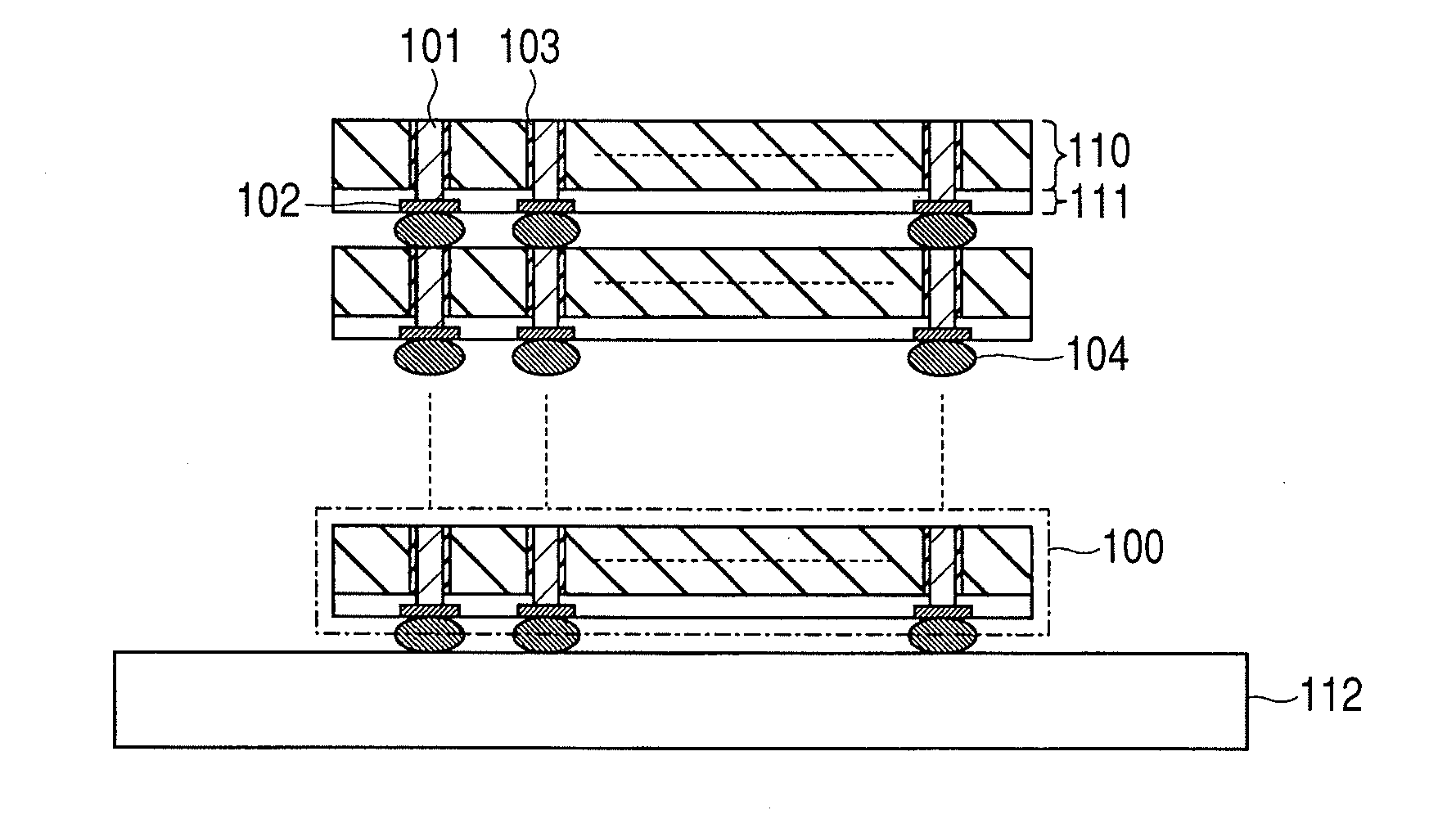
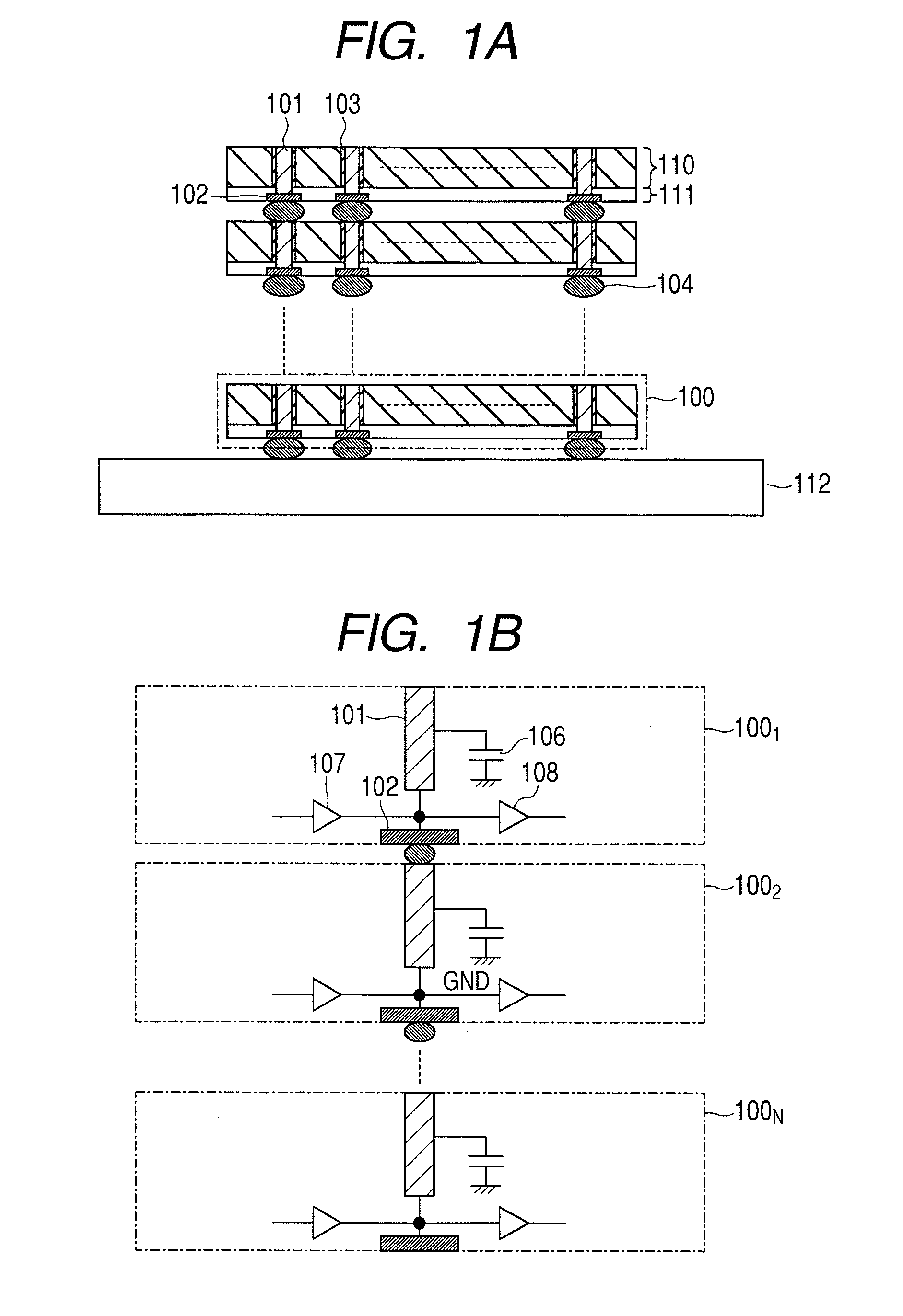
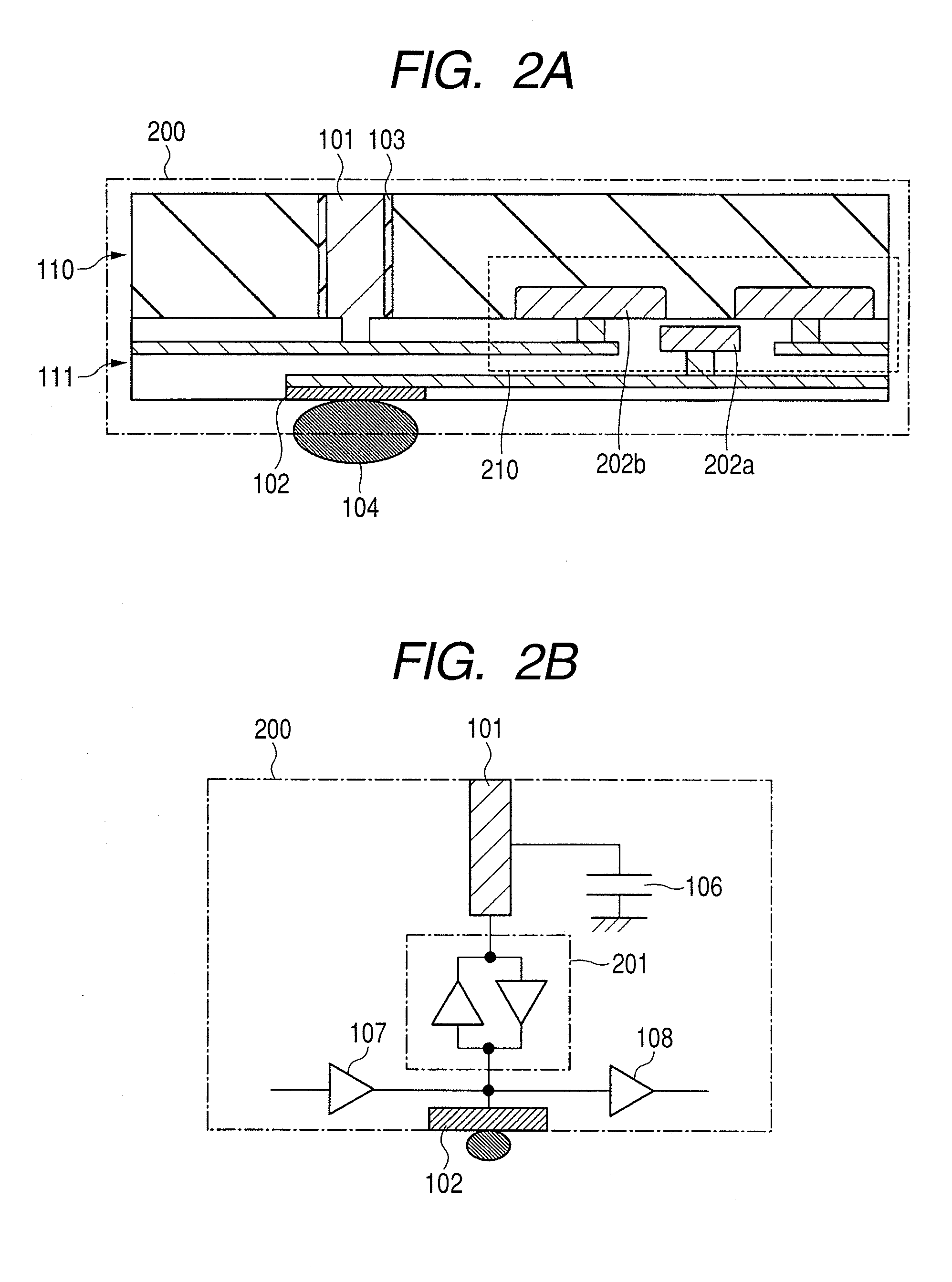
[0014]In FIG. 2B, the MOS transistor 210 of FIG. 2A is used as a portion of a repeater circuit (impedance converting circuit) 201. In respective semiconductor chips stacked to each other, by providing the repeater circuit 201, the parasitic capacitance 106 at the through-via-hole path can be partitioned for respective chips, and high speed communication among chips can be realized. The repeater circuit 201 is constituted by a unidirectional buffer circuit or a bidirectional buffer circuit in accordance with a specification of the transmitting direction. The unidirectional or bidirectional buffer circuit may preferably be constituted by a tristate buffer circuit. Thereby, a specific buffer circuit can be set to a high impedance state, for example, in the through-via-hole path, a portion of the path which is not used in a certain period of time can be divided, and wasteful power consumption in accordance with charging and discharging can be reduced. Incidentally, in FIG. 2B, the pad 102 is also connected with an input buffer circuit 108 for receiving a signal to a predetermined inner core circuit and an output buffer circuit 107 for transmitting a signal from the inner core circuit.

Problems solved by technology

A similar delay is caused also when the signal falls.
Therefore, an upper limit of a frequency of a high speed signal, for example, a clock signal in a rectangular wave shape is restricted.
However, when the data signal path is made to carry out the pipeline operation by using the latch circuit, although there is room for considerably improving a throughput of data transmission (that is, clock period), delay time (latency) is increased by clock period×stacked layer number, and therefore, the delay time is actualized as a big problem of latency particularly in stacking a CPU memory chip and a memory chip.
Furthermore, in JP-A-2006-330974, the clock signal still uses the through-via-hole of the background art, and therefore, actually, it is difficult to transmit high speed clock signal and the improvement in the through put described above can be limited.
Furthermore, addition of the parasitic capacitance effects a significant influence not only on the speed but the power consumption.
Although the circuit constitution is changed for the respective chips in the background art, a number of masks is increased, a kind of the chip formed is increased, and therefore, the circuit constitution is disadvantageous in view of design and fabrication cost.

Method used


Image

  • Semiconductor integrated circuit device
  • Semiconductor integrated circuit device
  • Semiconductor integrated circuit device

Examples


first embodiment

[0032]FIG. 3A is an equivalent circuit diagram of a semiconductor integrated circuit device according to a first embodiment of the invention showing an outline constitution example of an essential portion per one semiconductor chip 300 thereof, FIG. 3B is an equivalent circuit diagram showing a detailed constitution example of a repeater circuit in FIG. 3A, and FIG. 3C is an equivalent circuit diagram showing a through-via-hole path when the semiconductor chips 300 of FIG. 3A are mounted to stack. As shown by FIG. 3A, the semiconductor integrated circuit device of the first embodiment is essentially characterized in using a unidirectional buffer circuit 302 as a repeater circuit 301. In FIG. 3A, the pad 102 is connected to an input terminal of the buffer circuit 302 and the penetrated conductor 101 is connected to an output terminal of the buffer circuit302. Therefore, a signal is propagated from the downward pad 102 to the upward penetrated conductor 101.

[0033]The repeater circuit ...

second embodiment

[0036]FIG. 4A is an equivalent circuit diagram showing an outline constitution example of an essential portion per one semiconductor chip 400 in a semiconductor integrated circuit device according to a second embodiment of the invention, and FIG. 4B is an equivalent circuit diagram showing a through-via-hole path when the semiconductor chips 400 of FIG. 4A are mounted to stack. As shown by FIG. 4A, the semiconductor integrated circuit device of the second embodiment is essentially characterized in providing a unidirectional buffer circuit 402 which becomes a repeater circuit and providing a through bypass switch 403 connected in parallel between an input and an output of the buffer circuit 402 at a repeater circuit portion 401 attached with the switch of connecting the pad 102 and the penetrated conductor 101.

[0037]As described in first embodiment, by inserting the repeater circuits to all the semiconductor chips, a transmission frequency (that is, through put) of a signal is promot...

third embodiment

[0040]FIG. 5A is an equivalent circuit diagram showing an outline constitution example of an essential portion per one semiconductor chip 500 in a semiconductor integrated circuit device according to a third embodiment of the invention, and FIG. 5B is an equivalent circuit diagram showing a through-via-hole path when the semiconductor chips 500 of FIG. 5A are mounted to stack. As shown by FIG. 5A, the semiconductor integrated circuit device of the third embodiment is essentially characterized in using bidirectional buffer circuits 502, 503 in which one input is connected to other output as a repeater circuit 501. The respective buffer circuits 502, 503 are constituted by tristate buffers outputs of which can be set to a high impedance state. Therefore, a transmission direction of a signal of the through-via-hole path can be selected by, for example, activating one of the buffer circuits 502, 503 and deactivating other such that output becomes a high impedance state.

[0041]FIG. 6A sho...


PUM


Abstract

In a through-via-hole path of semiconductor chips stacked in N stages, repeater circuits are provided in the respective semiconductor chips. For example, a signal transmitted from an output buffer circuit of the semiconductor chip is transmitted to an input buffer circuit of the semiconductor chip via the repeater circuits of the respective semiconductor chips. The respective repeater circuits can isolate impedances on input sides and output sides, and therefore, a deterioration of a waveform quality accompanied by a parasitic capacitance parasitic on the through-via-hole path of the respective semiconductor chips can be reduced and a high speed signal can be transmitted.

Description

CLAIM OF PRIORITY[0001]The present application claims priority from Japanese patent application JP 2009-028037 filed on Feb. 10, 2009, the content of which is hereby incorporated by reference into this application.FIELD OF THE INVENTION[0002]The present invention relates to a semiconductor integrated circuit device. Particularly, in a semiconductor integrated circuit device stacking to mount semiconductor chips integrated with microprocessors, memories etc., the invention relates to a signal transmitting method among the respective semiconductor chips.BACKGROUND OF THE INVENTION[0003]For example, a significant characteristic of a CMOS (Complementary Metal Oxide Semiconductor) circuit resides in a scaling rule that when an element size is miniaturized, an increase in an operational speed and a reduction in power consumption can be realized. Heretofore, a degree of integration per chip and performance have been promoted by miniaturization of the element. However, with a progress in mi...

Claims


Application Information

Patent Timeline
IPC IPC(8): H01L23/538H01L25/16
CPCG11C5/04H01L25/0657H01L25/18H01L2224/16145H01L2225/06513H01L2225/06517H01L2924/13091H01L2225/06541H01L2924/01019H01L2924/00H01L2224/05009H01L2224/0557H01L2224/05001H01L2924/00014H01L2224/05571H01L2224/16146H01L2224/131H01L2224/05599H01L2224/05099H01L2924/014
Inventor FURUTA, FUTOSHIOSADA, KENICHISAEN, MAKOTO
Owner HITACHI LTD
Learn More