

Quantum interference device, atomic oscillator, and magnetic sensor
a quantum interference and atomic oscillator technology, applied in the field of quantum interference devices, atomic oscillators, magnetic sensors, can solve the problems of insufficient examination by taking into account, poor development yield per unit volume, and difficulty in reducing the size of cells, so as to improve the sensitivity and accuracy of every sensor, the effect of reducing the size of the sensor
- Summary
- Abstract
- Description
- Claims
- Application Information
AI Technical Summary
Benefits of technology
Problems solved by technology
Method used
Image

Examples
first embodiment
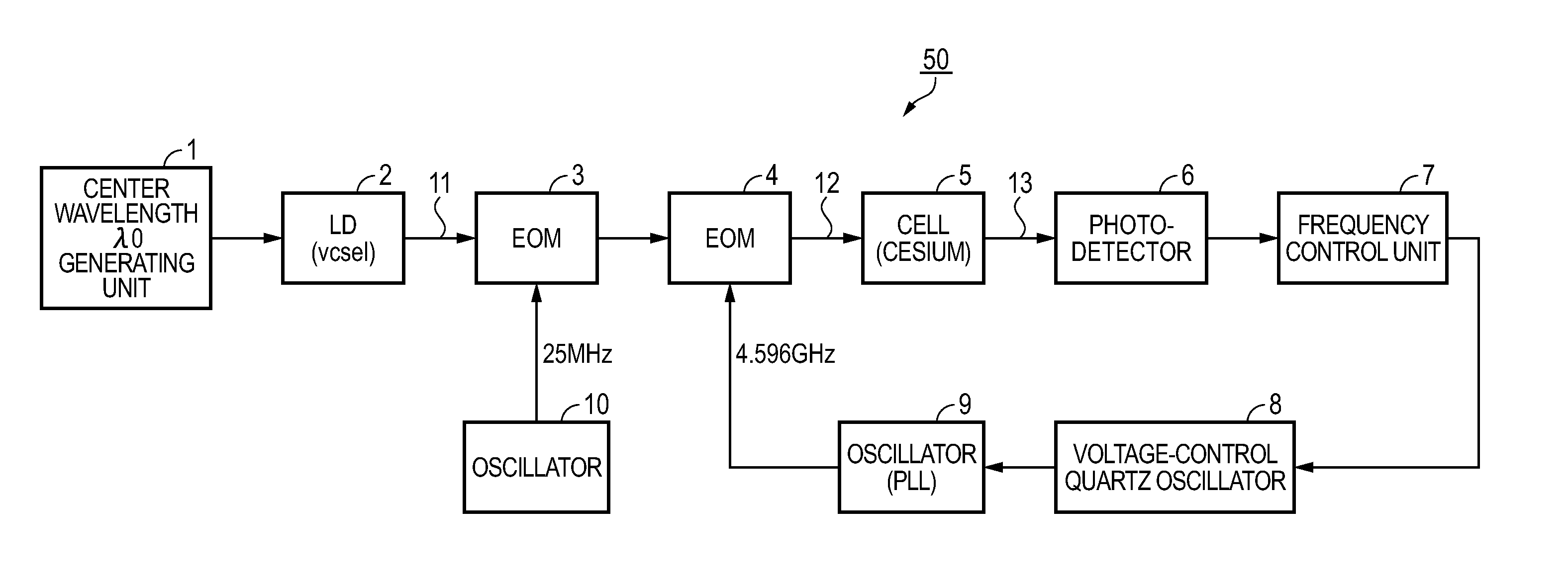
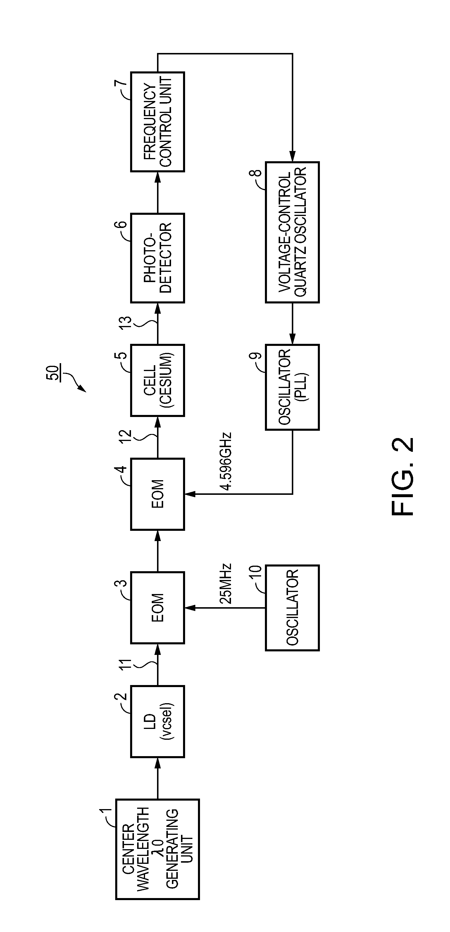
[0092]FIG. 2 is a block diagram of the configuration of an atomic oscillator according to the invention. An atomic oscillator 50 is an atomic oscillator that controls an oscillation frequency making use of a light absorption characteristic due to a quantum interference effect obtained when two or more pairs (three pairs as explained later) of resonant lights are made incident as coherent light pairs having different wavelengths. The atomic oscillator 50 includes an LD (VCSEL) (coherent light source) 2 that emits resonant lights, a center wavelength generating unit 1 that generates center wavelength of the LD 2, an oscillator 9 that oscillates a half (4.596 GHz) of a frequency (9.2 GHz) equivalent to an energy difference (ΔE12) between two different ground states, an oscillator 10 that oscillates a frequency of about 25 MHz, EOMs (electro-optical modulation elements) 3 and 4 that apply frequency modulation to resonant light 11 emitted from the LD 2 according to an electric signal, a ...
sixth embodiment
[0129]FIG. 22C is a diagram of an arrangement configuration of a cell, in which alkali metal atoms are encapsulated, a light source, an optical path, and a detector according to the invention. Light emitted from the laser light source is made incident on the cell and causes the EIT phenomenon with the alkali metal atoms. Then, the light folded via means such as reflection travels in the opposite direction to cause the EIT phenomenon with the alkali metal atoms in the cell again and is guided to the photodetector. This is a so-called reflection type. As shown in FIGS. 22A and 22B, when energy of an excitation level with Doppler width not taken into account is represented as E10, if excited energy Eend0 of single color light of the light source is selected not to be equal to E10 (E10<Eend0 or Eend0<E10), one resonant light pair can cause, in a forward path and a backward path, EIT with an alkali metal atom group having velocity components in opposite directions in the cell. Therefore,...
seventh embodiment
[0130]FIG. 23C is a diagram of an arrangement configuration of a cell, in which alkali metal atoms are encapsulated, a light source, an optical path, and a detector according to the invention. Light emitted from the laser light source is made incident on the cell and causes the EIT phenomenon with the alkali metal atoms. Then, the light passes through the cell plural times via means such as reflection, causes the EIT phenomenon every time the light passes through the cell, and is led to the photodetector. This is a so-called multiple reflection type. As shown in FIGS. 23A and 23B, if excited energy Eend of all plural resonant light pairs, which could cause the EIT phenomenon, is selected to satisfy only one of conditions Eend<E10 and E10<Eend, one resonant light pair can cause, in a forward path and a backward path, EIT with an alkali metal atom group having velocity components in opposite directions in the cell. Since optical path length is longer in the multiple reflection type, c...
PUM
 Abstract
Description
Claims
Application Information