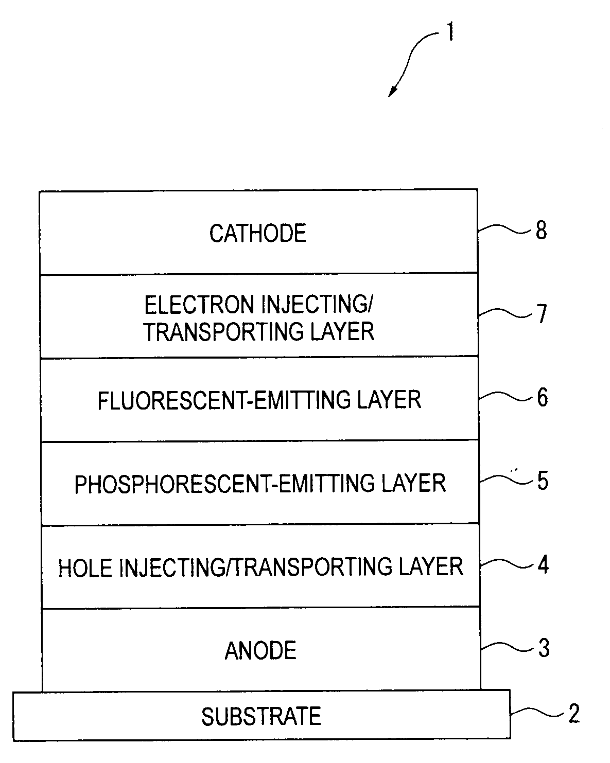
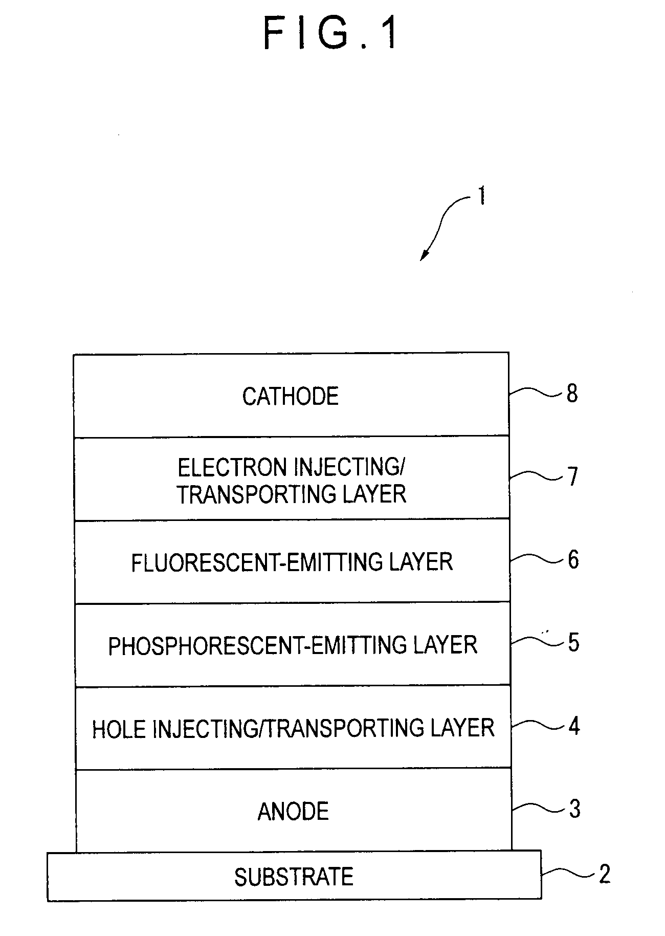
Organic el device

a technology of organic el and phosphorescent materials, which is applied in the field of organic el devices, can solve the problems of low luminous efficiency of fluorescent blue emission, inability to provide short-wavelength emission (blue emission) at a practical level, and difficulty in balancing the mixed color (e.g., white balance). achieve the effect of long life and high luminous efficiency

Active Publication Date: 2010-08-19
IDEMITSU KOSAN CO LTD
View PDF18 Cites 24 Cited by
  • Summary
  • Abstract
  • Description
  • Claims
  • Application Information

AI Technical Summary

Benefits of technology

[0011]An object of the invention is to solve the above problems and to provide a mixe

Problems solved by technology

However, a phosphorescent material capable of providing long-wavelength emission of green to red color has been known so far, but no phosphorescent material capable of providing short-wavelength emission (blue emission) at a practical level has been known.
However, while the quantum efficiency of the phosphorescent emission can be enhanced up to be 75% or more o

Method used


Image

  • Organic el device
  • Organic el device
  • Organic el device

Examples


example 1

[0213]A glass substrate (size: 25 mm×75 mm×1.1 mm thick) having an ITO transparent electrode (manufactured by Geomatec Co., Ltd.) was ultrasonic-cleaned in isopropyl alcohol for five minutes, and then UV / ozone-cleaned for 30 minutes.

[0214]After the glass substrate having the transparent electrode line was cleaned, the glass substrate was mounted on a substrate holder of a vacuum deposition apparatus. Then, 55-nm thick film of 4,4′-bis[N-(1-naphthyl)-N-phenylamino] biphenyl (hereinafter abbreviated as “NPD film”) was initially formed by resistance heating deposition onto a surface of the glass substrate where the transparent electrode line was provided in a manner of covering the transparent electrode. The NPD film served as the hole injecting / transporting layer.

[0215]A 5-nm thick film of CBP, which was used as the red phosphorescent host, was formed on the NPD film by resistance heating deposition. At the same time, the following compound (PD), which was used as the red phosphoresce...

example 2

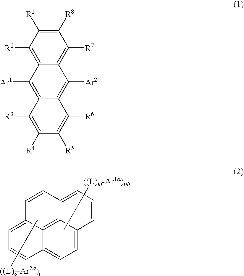
[0223]An organic EL device was manufactured in the same manner as Example 1, except that the following compound (AD2) was used as the fluorescent host in place of the compound (AD1).

example 3

[0224]An organic EL device was manufactured in the same manner as Example 1, except that the following compound (AD3) was used as the fluorescent host in place of the compound (AD1).


PUM

PropertyMeasurementUnit
Lengthaaaaaaaaaa
Wavelengthaaaaaaaaaa

Abstract

An organic EL device includes: an anode for injecting holes; a phosphorescent-emitting layer; a fluorescent-emitting layer; and a cathode for injecting electrons. The phosphorescent-emitting layer contains a phosphorescent host and a phosphorescent dopant for phosphorescent emission. The fluorescent-emitting layer contains a fluorescent host and a fluorescent dopant for fluorescent emission. The fluorescent host is at least one of an asymmetric anthracene derivative represented by a formula (1) below and a pyrene derivative represented by a formula (2) below.

Description

TECHNICAL FIELD[0001]The present invention relates to an organic EL device. In particular, the invention relates to an organic EL device including a fluorescent-emitting layer and a phosphorescent-emitting layer.BACKGROUND ART[0002]To date, organic EL devices including a plurality of emitting layers each of which emits light of a different wavelength are known. Such organic EL devices are also known to provide mixed-color light in which the lights emitted by the emitting layers are mixed together. One of such organic EL devices includes a layered red-emitting layer, green-emitting layer and blue-emitting layer, and provides white light in which emissions from the emitting layers are mixed together.[0003]In recent years, a further progress has been made in the development of phosphorescent materials utilizing the emission from triplet exciton energy, and devices of high luminous efficiency have been realized (e.g., Patent Document 1).[0004]Hence, some expect that devices for mixed-co...

Claims


Application Information

Patent Timeline
IPC IPC(8): H01L51/54
CPCC09K11/06C09K2211/1011C09B23/148C09B57/00C09B57/001C09B57/008C09B1/00C09B3/14C09B3/78H10K85/622H10K85/626H10K85/633H10K85/631H10K85/654H10K85/322H10K85/6572H10K85/657H10K85/324H10K85/342H10K50/125H10K50/11H10K2101/10H10K85/40H10K50/00
Inventor NISHIMURA, KAZUKIIWAKUMA, TOSHIHIROKAWAMURA, MASAHIROHOSOKAWA, CHISHIOFUKUOKA, KENICHIJINDE, YUKITOSHI
Owner IDEMITSU KOSAN CO LTD
Why Eureka
Try Eureka