Ultrafast magnetic recording element and nonvolatile magnetic random access memory using the magnetic recording element

a magnetic recording element and nonvolatile magnetic technology, applied in the field of magnetic recording elements, can solve the problems of loss of stored data, difficulty in achieving high integration, and difficulty in reading out information stored in the magnetic recording element, and achieve the effects of low power, accurate driving, and simple structur

Active Publication Date: 2010-08-19
SEOUL NAT UNIV R&DB FOUND
View PDF5 Cites 13 Cited by
  • Summary
  • Abstract
  • Description
  • Claims
  • Application Information

AI Technical Summary

Benefits of technology

[0021]According to a magnetic recording element in accordance with the present invention, a magnetic recording element having a simple structure can be realized using a magnetic layer with a magnetic vortex formed, and the magnetic recording element can be accurately driven with low power using a plurality of drive electrode pairs or a plurality of drive electrodes.
[0022]According to a magnetic ra

Problems solved by technology

However, typical dynamic random access memories (DRAMs) are volatile memory devices, and thus lose stored data when power is not supplied.
Also, the MRAM using the GMR effect may be affected by a magnetic field applied to adjacent magnetic recording elements, and thus the magnetic recording elements should be spaced apart from each other by a predetermined distance or more, leading to a difficulty in achieving high integration.
If, however, a thickness difference between an insulating layer of a storage magnetic recording element and an insula

Method used


Image

  • Ultrafast magnetic recording element and nonvolatile magnetic random access memory using the magnetic recording element
  • Ultrafast magnetic recording element and nonvolatile magnetic random access memory using the magnetic recording element
  • Ultrafast magnetic recording element and nonvolatile magnetic random access memory using the magnetic recording element

Examples


first embodiment

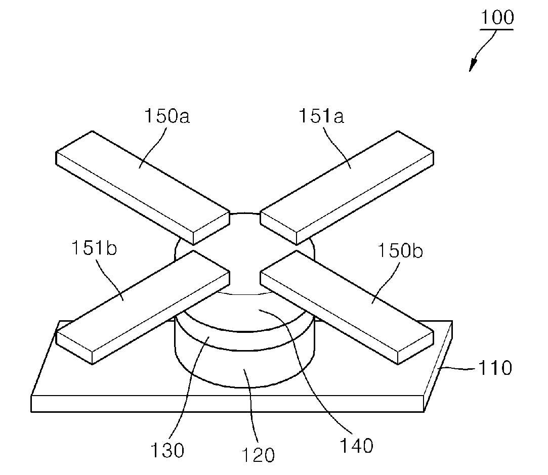
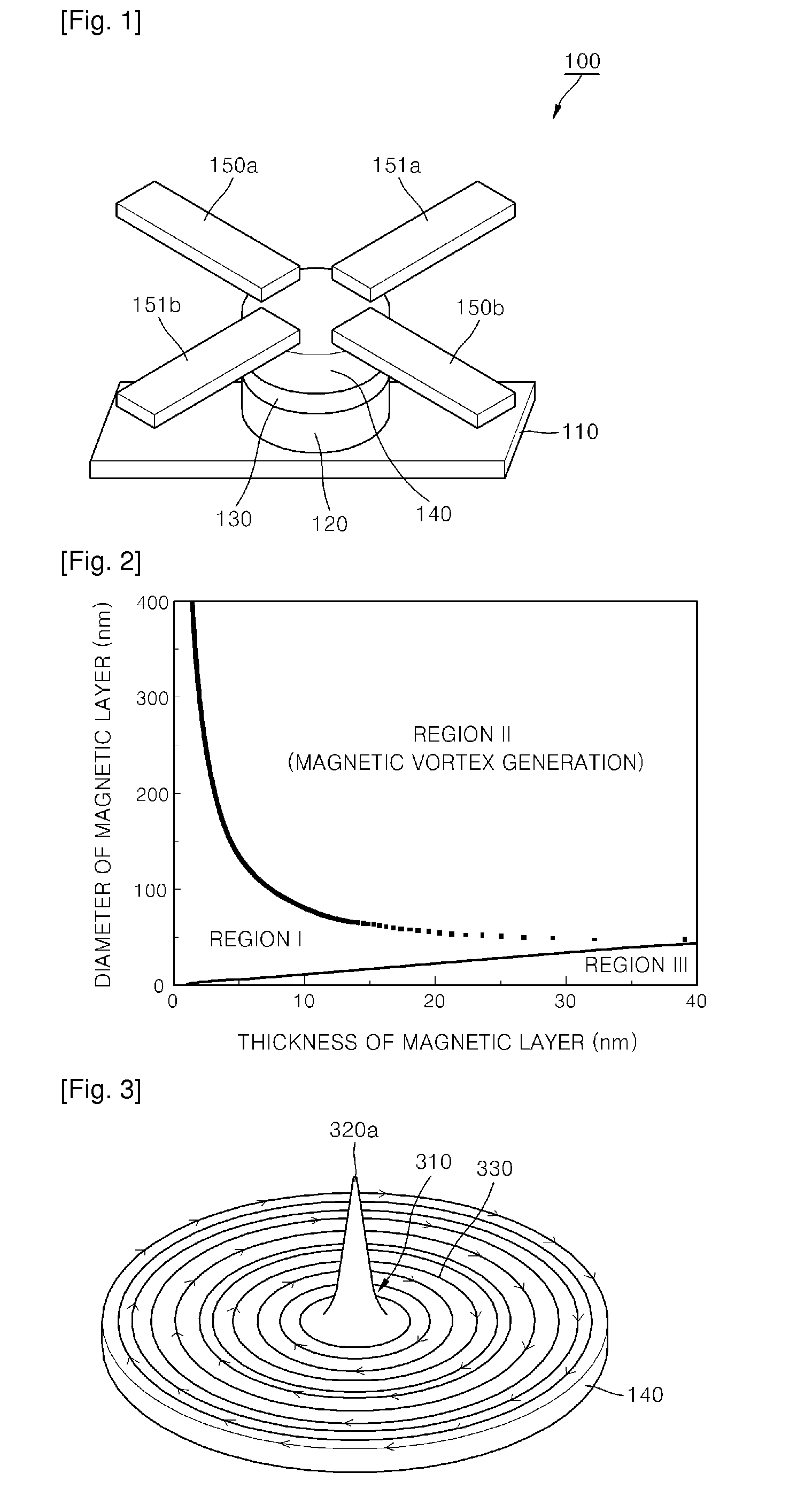
[0036]Referring to FIG. 1, the magnetic recording element 100 according to the present invention includes a read electrode 110, a magnetic pinned layer 120, an insulating layer 130, a magnetic free layer 140 and drive electrodes 150a, 150b, 151a and 151b.

[0037]The read electrode 110 is shaped in a plate extending in a direction, and is used for reading information stored in the magnetic recording element 100. The read electrode 110 may be formed of at least one of titanium (Ti), gold (Au), copper (Cu) and aluminum (Al), or a composite thereof. Desirably, the read electrode 110 may be composed of a bilayer of Ti and Au.

[0038]The magnetic pinned layer 120 is formed in a plate shape on the read electrode 110. The magnetic pinned layer 120 may be formed in a disk shape. The magnetic pinned layer 120 may be formed of at least one of cobalt (Co), iron (Fe), nickel (Ni), Fe—Ni alloy (i.e., permalloy), Fe—Co (i.e., permendur), Fe—Ni—Co alloy (perminvar), Fe—Ni—Mo alloy (i.e., supermalloy)....

second embodiment

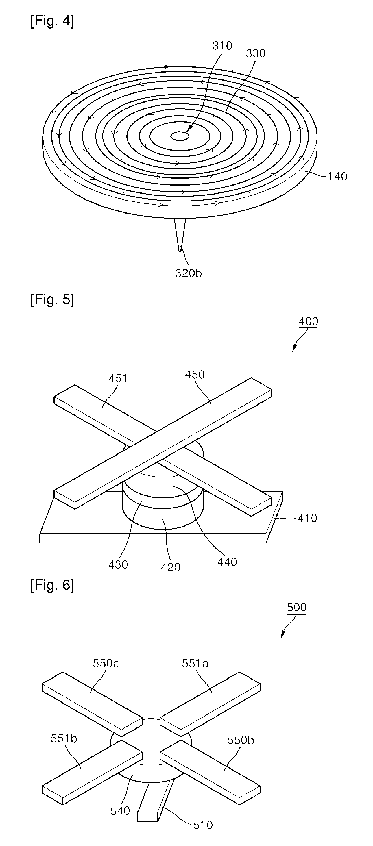
[0070]Referring to FIG. 5, the magnetic recording element 400 according to the present invention includes a read electrode 410, a magnetic pinned layer 420, an insulating layer 430, a magnetic free layer 440 and drive electrodes 450 and 451.

[0071]The read electrode 410, the magnetic pinned layer 420, the insulating layer 430, and the magnetic free layer 440 correspond to the read electrode 110, the magnetic pinned layer 120, the insulating layer 130 and the magnetic free layer 140 included in the magnetic recording element 100 illustrated in FIG. 1, respectively. In the magnetic recording element 400 of FIG. 5, information is also stored in a core orientation of a magnetic vortex formed in the magnetic free layer 440.

[0072]The drive electrodes 450 and 451 included in the magnetic recording element 400 of FIG. 5 may be formed in plurality such that they cross each other while covering a central portion of the top surface of the magnetic free layer 440. Desirably, the two drive electr...

third embodiment

[0076]Referring to FIG. 6, a magnetic recording element 500 according to the present invention includes a magnetic free layer 540, drive electrodes 550a, 550b, 551a and 551b, and a read line 510.

[0077]The magnetic free layer 540 and the drive electrodes 550a, 550b, 551a and 551b included in the magnetic recording element 500 of FIG. 6 respectively correspond to the magnetic free layer 140 and the drive electrodes 150a, 150b, 151a and 151b included in the magnetic recording element 100 in FIG. 1. In the magnetic recording element 500 of FIG. 6, information is also stored in a core orientation of a magnetic vortex formed in the magnetic free layer 540.

[0078]The read line 510 included in the magnetic recording element 500 of FIG. 6 extends in a direction and disposed around the magnetic free layer 540. When a predetermined voltage is applied to the magnetic free layer 540 through the drive electrodes 550a, 550b, 551a and 551b, the magnetic vortex core formed in the magnetic free layer ...


PUM


Abstract

Provided are an ultrafast magnetic recording element and a nonvolatile magnetic random access memory using the same. The magnetic recording element includes a read electrode, a magnetic pinned layer formed on the read electrode, and an insulating layer or a conductive layer formed on the magnetic pinned layer. The magnetic recording element includes a magnetic free layer formed on the insulating layer or the conductive layer, in which a magnetic vortex is formed, and a plurality of drive electrodes applying a current or magnetic field to the magnetic free layer. Alternatively, the magnetic recording element includes a magnetic free layer in which a magnetic vortex is formed, a plurality of drive electrodes applying a current or a magnetic field to the magnetic free layer, and a read line disposed around the magnetic free layer. Herein, a current generated by a voltage induced by the movement of a magnetic vortex core flows through the read line. According to the magnetic recording elements, the magnetic recording element with a simple structure can be realized using a magnetic layer with a magnetic vortex formed, and the magnetic recording element can be accurately driven with low power using a plurality of drive electrodes.

Description

TECHNICAL FIELD [0001]The present invention relates to a magnetic recording element available in a nonvolatile random access memory, and more particularly, to a magnetic recording element using a magnetic vortex existing in a magnetic layer of a few micrometers in size.BACKGROUND ART [0002]In line with remarkable developments in an information and telecommunication field, there is an increasing demand for various kinds of memory devices. In particular, nonvolatile memory devices, which can retain data even if power is turned off, are demanded as memory devices available for mobile terminals, MP3 players, or the like. Since nonvolatile memory devices can electrically program and erase data, and retain data even though power is not supplied, they are increasingly applied to a variety of fields at present. However, typical dynamic random access memories (DRAMs) are volatile memory devices, and thus lose stored data when power is not supplied. Therefore, many studies are being conducted...

Claims


Application Information

Patent Timeline
IPC IPC(8): H01L29/82
CPCG11C11/155H01L43/08H01L27/222H10B61/00H10N50/10
Inventor KIM, SANG-KOOGLEE, KI-SUKYU, YOUNG-SANG
Owner SEOUL NAT UNIV R&DB FOUND
Why Eureka
Try Eureka