

Extreme ultraviolet light source apparatus
a light source and ultraviolet light technology, applied in the field of extreme ultraviolet light source equipment, can solve the problems of reducing the reflectance ratio of optical elements, erode the surface of optical elements with high energy, and damage the reflective coating of surfaces,
- Summary
- Abstract
- Description
- Claims
- Application Information
AI Technical Summary
Problems solved by technology
Method used
Image

Examples
first embodiment
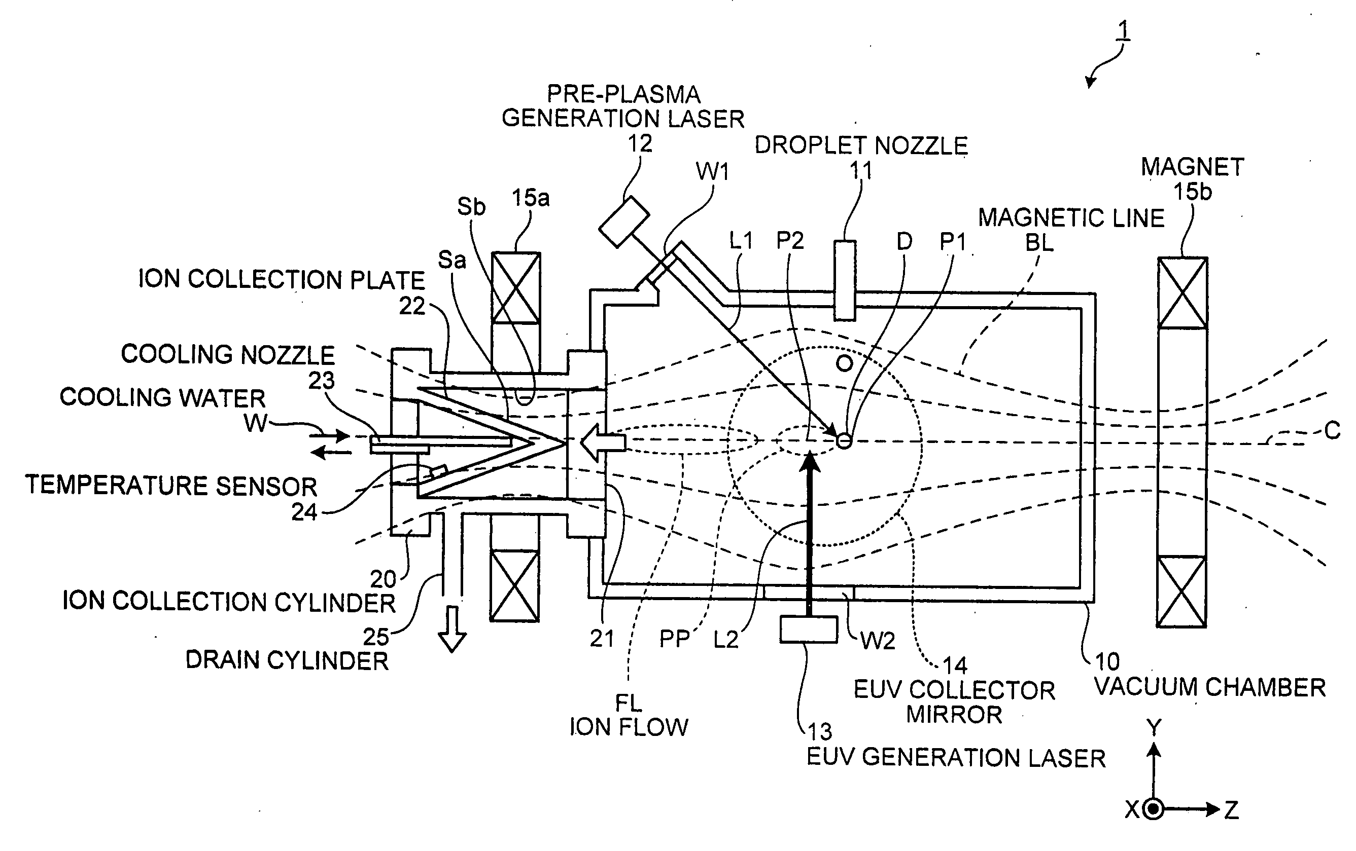
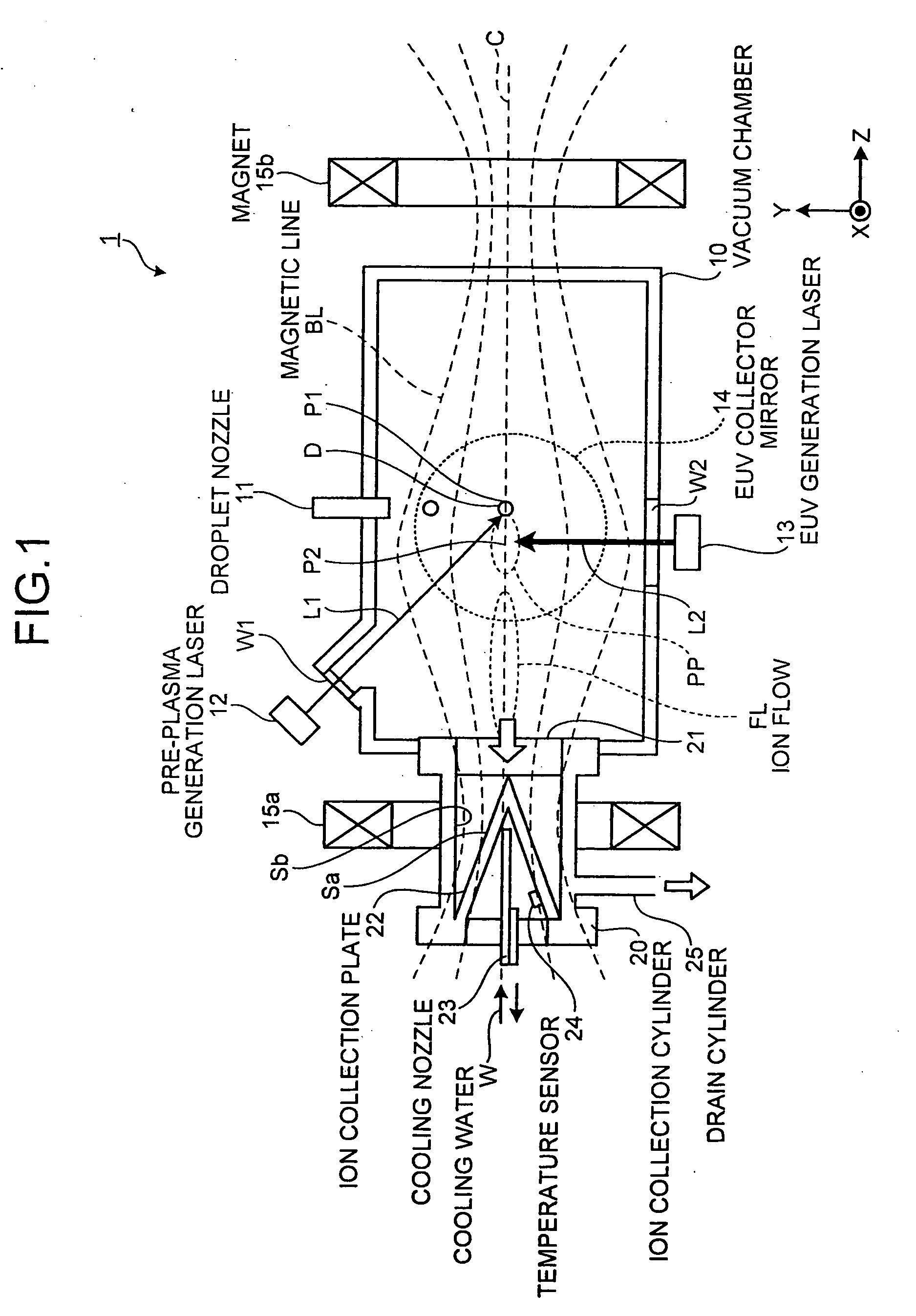
[0038]FIG. 1 is a sectional view of an extreme ultraviolet light source apparatus according to a first embodiment of the present invention. In FIG. 1, an extreme ultraviolet light source apparatus 1 includes a vacuum chamber 10. A droplet nozzle 11 ejects a droplet D of molten Sn into the vacuum chamber 10. A pre-plasma generation laser 12, which is a YAG pulse laser, is arranged outside the vacuum chamber 10. A pre-plasma generation laser light L1 outputted from the pre-plasma generation laser 12 enters the vacuum chamber 10 via a window W1, and hits a part of the droplet D ejected from the droplet nozzle 11 at position P1 which is substantially at the center of the vacuum chamber 10. As a result, pre-plasma PP is generated in −Z direction. Herein, “pre-plasma” refers to a state of plasma, or a state of mixture of plasma and steam.
[0039]Furthermore, an EUV generation laser 13, which is a CO2 pulse laser, is arranged outside the vacuum chamber 10. An EUV generation laser light L2 ou...
second embodiment
[0053]In the first embodiment described above, the multi-step irradiation including the process for generating the pre-plasma is adopted for the reduction of initial energy of Sn ion. In a second embodiment, a mass-limited target is employed as a target for the reduction of initial energy of a target atom discharged as debris. Here, “mass-limited target” refers to a target which has a minimum required mass for generating a desirable EUV light. For example, a mass-limited target illustrated in FIG. 9 is a droplet D1 having a diameter of 10 μm. The intensity of the EUV generation laser light can thus be lowered, and as a result, the initial energy of generated Sn ion can be lowered. Specifically, Sn density has to be about 1 to 5×1018 cm−3 for EUV light conversion efficiency of 4%. To satisfy this condition, it is sufficient if the diameter of the droplet D1 of a liquid Sn ejected from a nozzle 11a is 10 μm. When the diameter of the droplet D1 is 10 μm, a required power of the EUV gen...
third embodiment
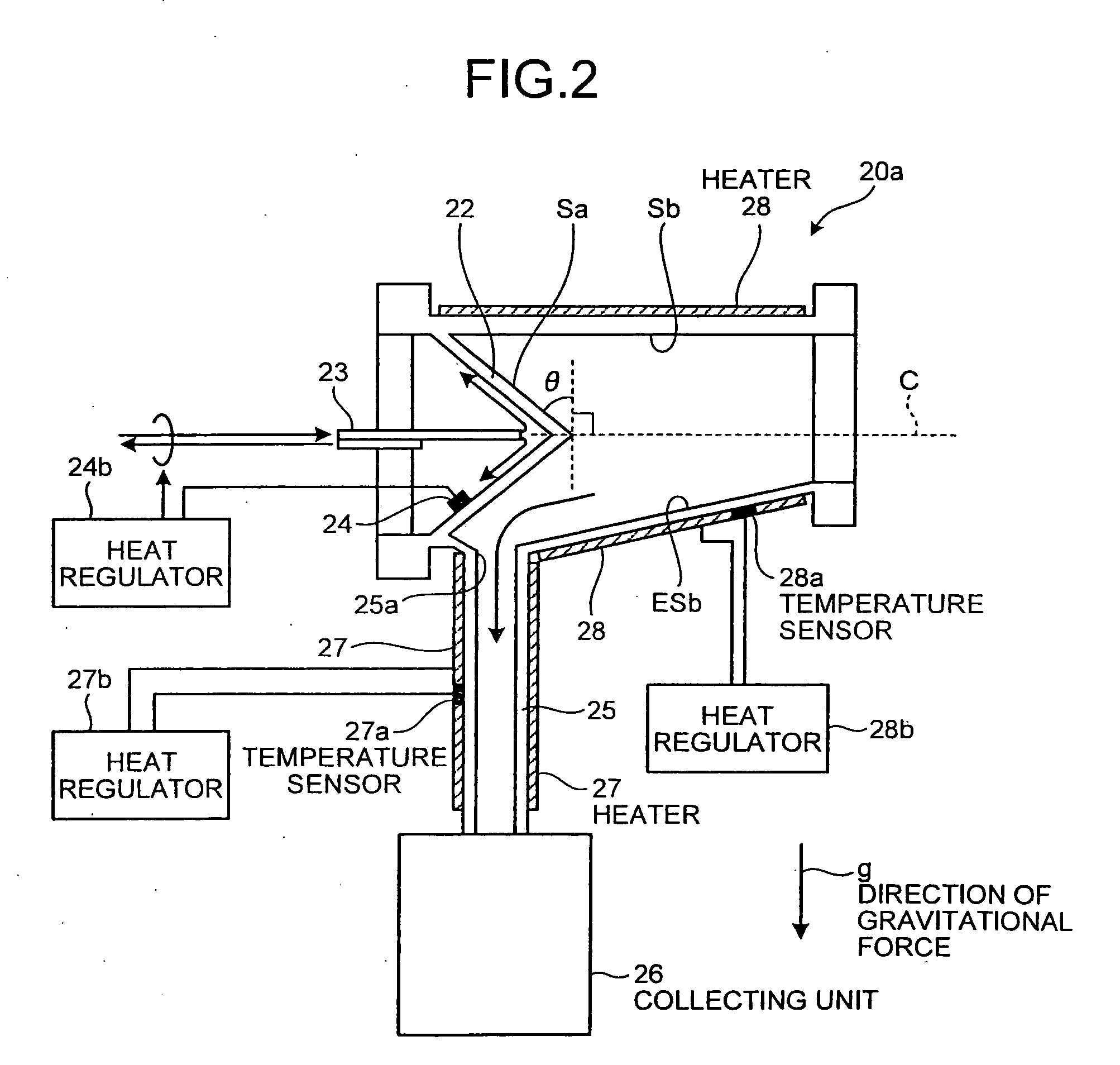
[0056]A third embodiment of the present invention will be described. FIG. 12 is a sectional view illustrating a configuration of an extreme ultraviolet light source apparatus according to the third embodiment of the present invention. In the third embodiment, a pair of mutually opposing ion collection cylinders 30a and 30b is arranged on the central axis C of the magnetic field. The pair of ion collection cylinders 30a and 30b collects Sn ion which converges along the central axis C of the magnetic field and moves as ion flows FL1 and FL2. The ion collection cylinders 30a and 30b respectively include grounded grid electrodes 33a and 33b arranged at the side of incident Sn ion and ion collection plates 32a and 32b arranged at the bottom side and to which a high positive potential is applied. With this configuration, the velocity of incoming Sn ion is decreased by an electric field E applied between the grid electrode 33a and the ion collection plate 32a and between the grid electrode...
PUM
 Abstract
Description
Claims
Application Information