Apparatus having thermal-enhanced and cost-effective 3D IC integration structure with through silicon via interposers

a technology of integrated circuits and interposers, which is applied in the direction of electrical apparatus, semiconductor devices, semiconductor/solid-state device details, etc., can solve the problems of bt substrates no longer supporting, build-up layers, and great challenges, and achieve the effect of improving thermal management and low cos

Active Publication Date: 2010-08-26
THE HONG KONG UNIV OF SCI & TECH
View PDF17 Cites 102 Cited by
  • Summary
  • Abstract
  • Description
  • Claims
  • Application Information

AI Technical Summary

Benefits of technology

[0016]This specification describes a three-dimensional integrated circuit (3D IC) struc...

Problems solved by technology

Unfortunately, conventional substrates with build-up layers made up of organic materials, e.g., bismaleimide triazine (BT), are facing great challenges in supporting these high pin-count, fine-pitched silicon chips.
As the chip gets bigger with a higher pin count and finer pitch, the BT substrate can no longer support it.
However, due to high density and high complexity of the circuit components, it is difficult to dispose TSV on the active circuit dies and wafers.
Therefore, forcing them tog...

Method used


Image

  • Apparatus having thermal-enhanced and cost-effective 3D IC integration structure with through silicon via interposers
  • Apparatus having thermal-enhanced and cost-effective 3D IC integration structure with through silicon via interposers
  • Apparatus having thermal-enhanced and cost-effective 3D IC integration structure with through silicon via interposers

Examples


Embodiment Construction

[0030]In order to achieve the objectives described above, the 3D IC integration structure utilizes a TSV interposer for providing chip-to-chip interconnections. As described in various embodiments below with reference to the drawings, the structure can be integrated into a 3D System-in-Package (SiP) format to provide improved thermal management.

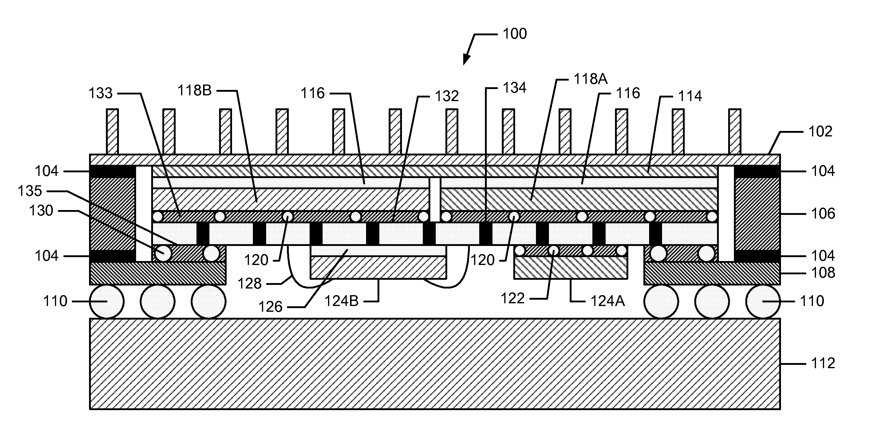
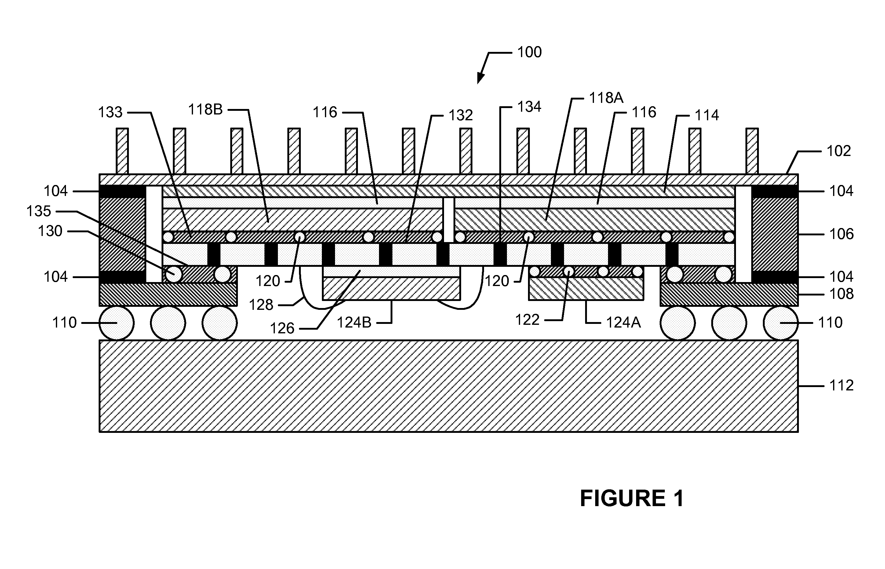
[0031]Now turning to FIG. 1, depicted therein is 3D IC apparatus 100 including interposer 132 for supporting high-power chips 118A and 118B and low-power chips 124A and 124B. The apparatus 100 includes a standard face-down PBGA package attached printed circuit board 112.

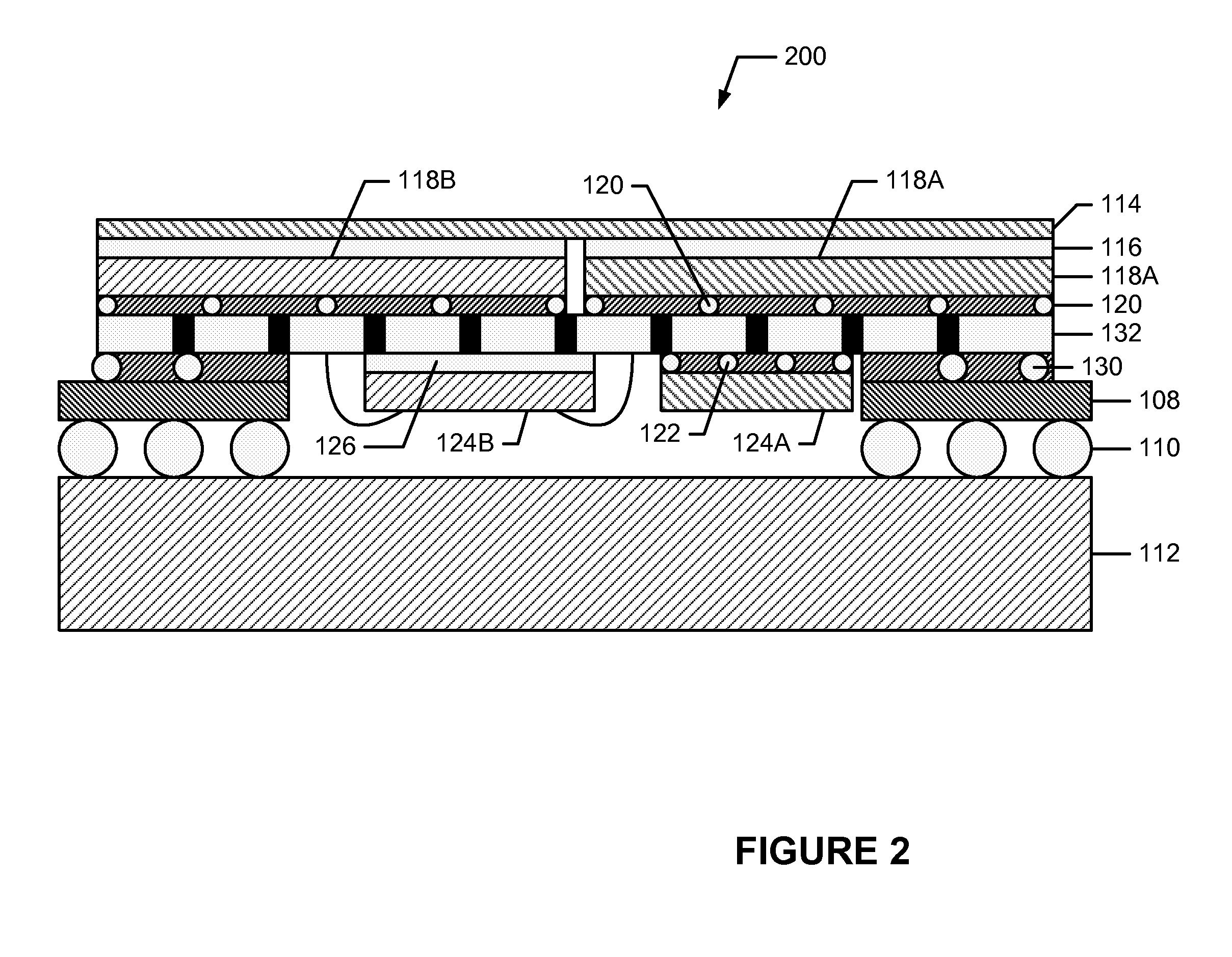
[0032]In particular, the interposer 132 includes high-density TSVs 134 and redistribution layers to connect the high-power chips 118A and 118B and low-power chips 124A and 124B. The interposer 132 provides signal redistributions among the high and low-power chips. The interposer 132 has conductive metal pads of different sizes and at different locations on its top and bottom s...


PUM


Abstract

An apparatus having a three-dimensional integrated circuit structure is described herein. The apparatus include an interposer for carrying a plurality of high and low-power chips. The high-power chips are attached and connected to one side of the interposer, while the low-power chips are attached and connected to the other side of the interposer. In generally, the high-power chips produce more heat than does the low-power chip during their operations. The interposer further include through silicon vias and redistribution layers for connecting the chips on both surfaces. In addition, the interposer assembly is attached and connected to a substrate layer, which is in turn attached and connected to a printed circuit board. In order to provide improve thermal management, the interposer surface carrying the high-power chips are oriented away from the circuit board. A heat spreader is attached to the back sides of the high-power chips for dissipating the heat.

Description

CROSS-REFERENCE TO RELATED APPLICATION[0001]This patent application claims the benefit of U.S. Provisional Patent Application No. 61 / 202,347, filed Feb. 20, 2009, which is incorporated by reference in its entirety.TECHNICAL FIELD[0002]The present invention relates in general to integrated circuit (IC) structures and in particular to a high-performance structural design for three-dimensional system in package (SiP) with improved thermal management.BACKGROUND OF THE INVENTION[0003]Moore's law has been the most powerful driver for the development of the microelectronic industry. This law emphasizes lithography scaling and conventional two-dimensional integration of all functions on a single chip, often called system-on-chip (SoC). On the other hand, the integration of all system components can be achieved through system-in-package (SiP) and, ultimately, through three-dimensional IC integration and packaging.[0004]A system-in-a-package includes a number of integrated circuits enclosed i...

Claims


Application Information

Patent Timeline
IPC IPC(8): H01L23/34H01L21/60H01L23/498
CPCH01L23/055H01L23/433H01L23/5384H01L23/5385H01L24/16H01L24/32H01L24/48H01L24/73H01L25/0652H01L25/18H01L2224/16225H01L2224/32H01L2224/32245H01L2224/48091H01L2224/48225H01L2224/48235H01L2224/73204H01L2224/73253H01L2224/73265H01L2225/0651H01L2225/06517H01L2225/06548H01L2225/06572H01L2225/06589H01L2924/14H01L2924/1432H01L2924/1433H01L2924/14335H01L2924/1434H01L2924/1436H01L2924/1437H01L2924/1461H01L2924/15153H01L2924/1517H01L2924/15311H01L2924/1532H01L2924/19041H01L2924/19043H01L2924/19105H01L2924/19106H01L2924/01019H01L2224/32225H01L2224/48227H01L2924/10253H01L2924/00014H01L2924/00H01L2924/00011H01L2224/0401H01L2224/45099H01L2224/45015H01L2924/207
Inventor LAU, HON SHINGLEE, SHI-WEIYUEN, MATTHEW MING FAIWU, JINGSHENLO, CHI CHUENFAN, HAIBOCHEN, HAIBIN
Owner THE HONG KONG UNIV OF SCI & TECH
Why Eureka
Try Eureka