Semiconductor Device and Driving Method Thereof, and Electronic Device

a technology of semiconductor devices and driving methods, applied in the direction of instruments, computing, electric digital data processing, etc., can solve the problems of insufficient compensation of mobility variation, inability to accurately process, and inability to perform accurate processes, so as to reduce the influence of threshold voltage of transistor variation, and reduce the influence of current characteristic variation

Inactive Publication Date: 2010-09-02
SEMICON ENERGY LAB CO LTD
View PDF23 Cites 37 Cited by
  • Summary
  • Abstract
  • Description
  • Claims
  • Application Information

AI Technical Summary

Benefits of technology

[0056]An embodiment of the present invention can reduce influence of variation in threshold voltage of a transistor. Alternatively, an embodiment of the present invention can reduce influence of variation in mobility of a transistor. Alternatively, an embodiment of the present invention can reduce influence of variation of current characteristic of a transistor. Alternatively, an embodiment of the present invention can obtain a long inputting period of an image signal. Alternatively, an embodiment of the present invention can obtain a long compensation period for reducing influence of variation in threshold voltage. Alternatively, an embodiment of the present invention can obtain a long compensation period for reducing...

Problems solved by technology

In techniques disclosed in Patent Documents 7 and 8, variation in mobility of a transistor is compensated while an image signal (a video signal) is input to a pixel, so that problems occur.
As a result, accurate processes cannot be performed because of lack of processing period, or compensation of variation in mobility is insufficient because the period in which variation in mobility is compensated is ...

Method used


Image

  • Semiconductor Device and Driving Method Thereof, and Electronic Device
  • Semiconductor Device and Driving Method Thereof, and Electronic Device
  • Semiconductor Device and Driving Method Thereof, and Electronic Device

Examples


embodiment 1

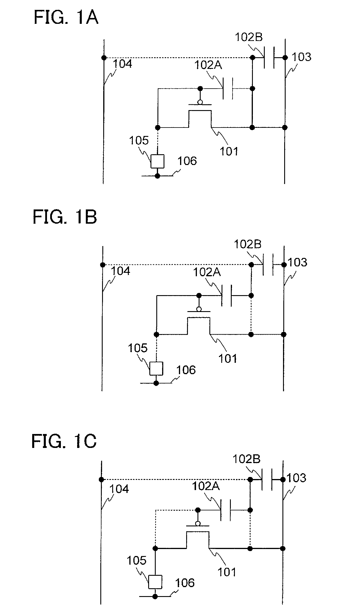
[0082]FIGS. 1A to 1C show an example of a driving method, driving timing, and a circuit structure in the case of compensating variation in current characteristics such as threshold voltage of a transistor or mobility. Note that in this embodiment, description is made about a transistor having p-type conductivity as an example.

[0083]A circuit structure in the period for compensating variation in threshold voltage of a transistor 101 is shown in FIG. 1A. That is, a circuit structure in the period in which a capacitor holds charge corresponding to the threshold voltage of the transistor 101 in a capacitor connected to the transistor 101 is shown. Note that the circuit structure shown in FIG. 1A is a circuit structure for discharging charge held in a gate of the transistor, and actually realizes a connection relation in the circuit structure by controlling on / off of a plurality of switches provided between wirings. Note that in the diagram, a solid line shows a conduction state between ...

embodiment 2

[0136]This embodiment will be described a specific example of the circuit and driving method described in Embodiment 1.

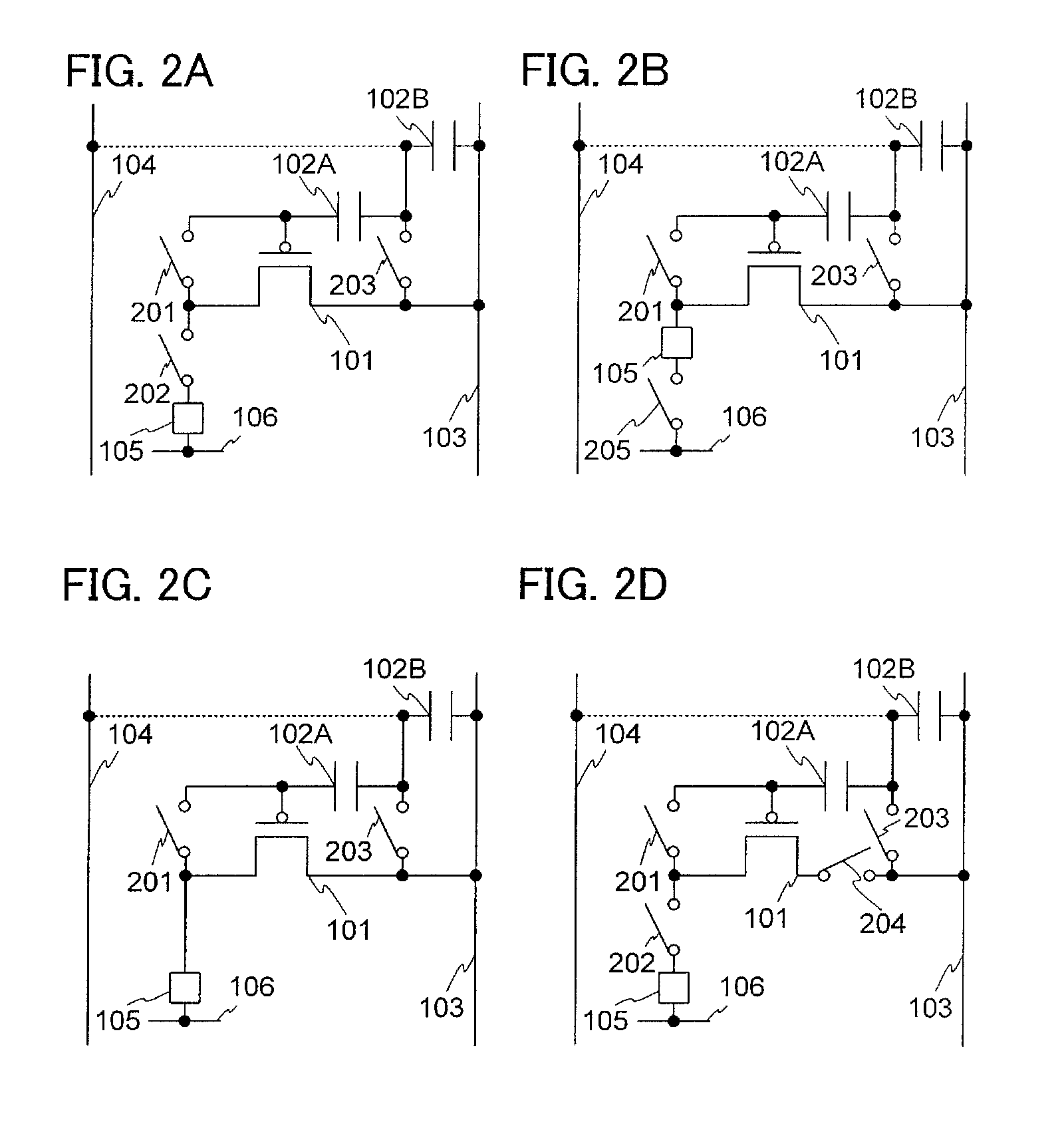
[0137]A specific example of the circuit structure described in Embodiment 1 is illustrated in FIGS. 8A to 8F. A first terminal of a switch 601 is connected to the wiring 104. A second terminal of the switch 601 is connected to the second terminal of the capacitor 102A, the first terminal of the capacitor 102B, and the first terminal of the switch 203. The second terminal of the switch 203 is connected to the wiring 103 and the first terminal of the transistor 101. The first terminal of the capacitor 102A is connected to the gate of the transistor 101 and a first terminal of the switch 201. The second terminal of the transistor 101 is connected to the second terminal of the switch 201 and a first terminal of the switch 202. The second terminal of the switch 202 is connected to the first terminal of the display element 105. A second terminal of the display element 105...

embodiment 3

[0160]In this embodiment, another specific example or deformation example of the circuit and driving method which are described in Embodiment 1.

[0161]Specific examples of FIGS. 1A to 1C, FIG. 9C, and FIG. 10C are illustrated in FIG. 11A. FIG. 11A shows a wiring 1101, a wiring 1102, a wiring 1103, a wiring 1104, a capacitor 1105, a transistor 1106, a transistor 1107, and a display element 1108. Note that the wiring 1101 corresponds to the wiring 103 of FIG. 9C. The wiring 1102 corresponds to the wiring 106 of FIG. 9C. Note that the wiring 1104 corresponds to the wiring 104 in FIG. 9C. Note that the capacitor 1105 corresponds to the capacitor 102B of FIG. 9C. Note that the transistor 1106 corresponds to the transistor 101 of FIG. 9C. The transistor 1107 corresponds to the display element 105 of FIG. 9C. Note that the transistors 1106 and 1107 are p-channel transistors in description below. Note that description will be made by using an EL element as an example of a display element.

[01...


PUM


Abstract

A driving method of a semiconductor device for compensating variation in threshold voltage and mobility of a transistor is provided. A driving method of a semiconductor device including a transistor and a capacitor electrically connected to a gate of the transistor includes a first period where voltage corresponding to threshold voltage of the transistor is held in the capacitor, a second period where a total voltage of video signal voltage and threshold voltage is held in the capacitor holding the threshold voltage, and a third period where charge held in the capacitor in accordance with the total voltage of the video signal voltage and the threshold voltage in the second period is discharged through the transistor.

Description

BACKGROUND OF THE INVENTION[0001]1. Field of the Invention[0002]The present invention relates to a semiconductor device, a display device, or a light-emitting device, or a driving method thereof.[0003]2. Description of the Related Art[0004]Flat panel displays such as liquid crystal displays (LCD) become widely used in recent years. However, LCDs have various drawbacks such as a narrow viewing angle, narrow chromaticity range, and slow response speed. Thus, to overcome those drawbacks, research of an organic EL (also referred to as an electroluminescence, an organic light-emitting diode, an OLED, or the like) displays have been actively conducted (Patent Document 1).[0005]However, organic EL displays have a problem in which current characteristics of transistors for controlling current which flows into organic EL elements vary from pixel to pixel. When current flowing into the organic EL elements (that is, current flowing into the transistors) varies, luminance of the organic EL elem...

Claims


Application Information

Patent Timeline
IPC IPC(8): G06F3/038
CPCG09G3/3233G09G2300/0819G09G2300/0852G09G3/22G09G2310/0251G09G2320/0233G09G2320/045G09G2300/0876G09G2300/0426G09G2330/021
Inventor KIMURA, HAJIME
Owner SEMICON ENERGY LAB CO LTD
Why Eureka
Try Eureka