Insulated Gate-Type Semiconductor Device and Manufacturing Method Thereof

a gate-type semiconductor and gate-type technology, applied in the direction of semiconductor devices, basic electric elements, electrical appliances, etc., can solve the problems of delay in hole supply, low on-resistance state, and large quantity of holes to be supplied, so as to achieve the effect of reducing the withstand voltage and good on-resistance characteristics

Active Publication Date: 2010-09-09
DENSO CORP
View PDF3 Cites 75 Cited by
  • Summary
  • Abstract
  • Description
  • Claims
  • Application Information

AI Technical Summary

Benefits of technology

[0024]The drift region has a low concentration region kept in contact with the body region and a high concentration region disposed below the low concentration region. The lower face of the high concentration region is positioned below the lower end of the floating diffusion region. Hence, with another insulated gate-type semiconductor device of the invention, a depletion layer is unlikely to spread below the floating diffusion region when the gate voltage is off. As a result, since the depletion layer does not originally spread over a wide range at the time of the gate voltage being off, the drift current is not impeded when the gate voltage is turned on. Accordingly, a good on-resistance characteristic is obtained. Moreover, a low concentration region is provided between the high concentration region and the body region. In doing so, a withstand voltage can be held by means of a depletion layer spreading mainly from the lower face of the body region, thereby suppressing a lowering of

Problems solved by technology

This results in operation in a low on-resistance state.
However, the insulated gate-type semiconductor device having such a floating structure as set out hereinabove is more unlikely to return to the low on-resistance state when stayed at C in FIG. 26 in comparison with an

Method used


Image

  • Insulated Gate-Type Semiconductor Device and Manufacturing Method Thereof
  • Insulated Gate-Type Semiconductor Device and Manufacturing Method Thereof
  • Insulated Gate-Type Semiconductor Device and Manufacturing Method Thereof

Examples


first embodiment

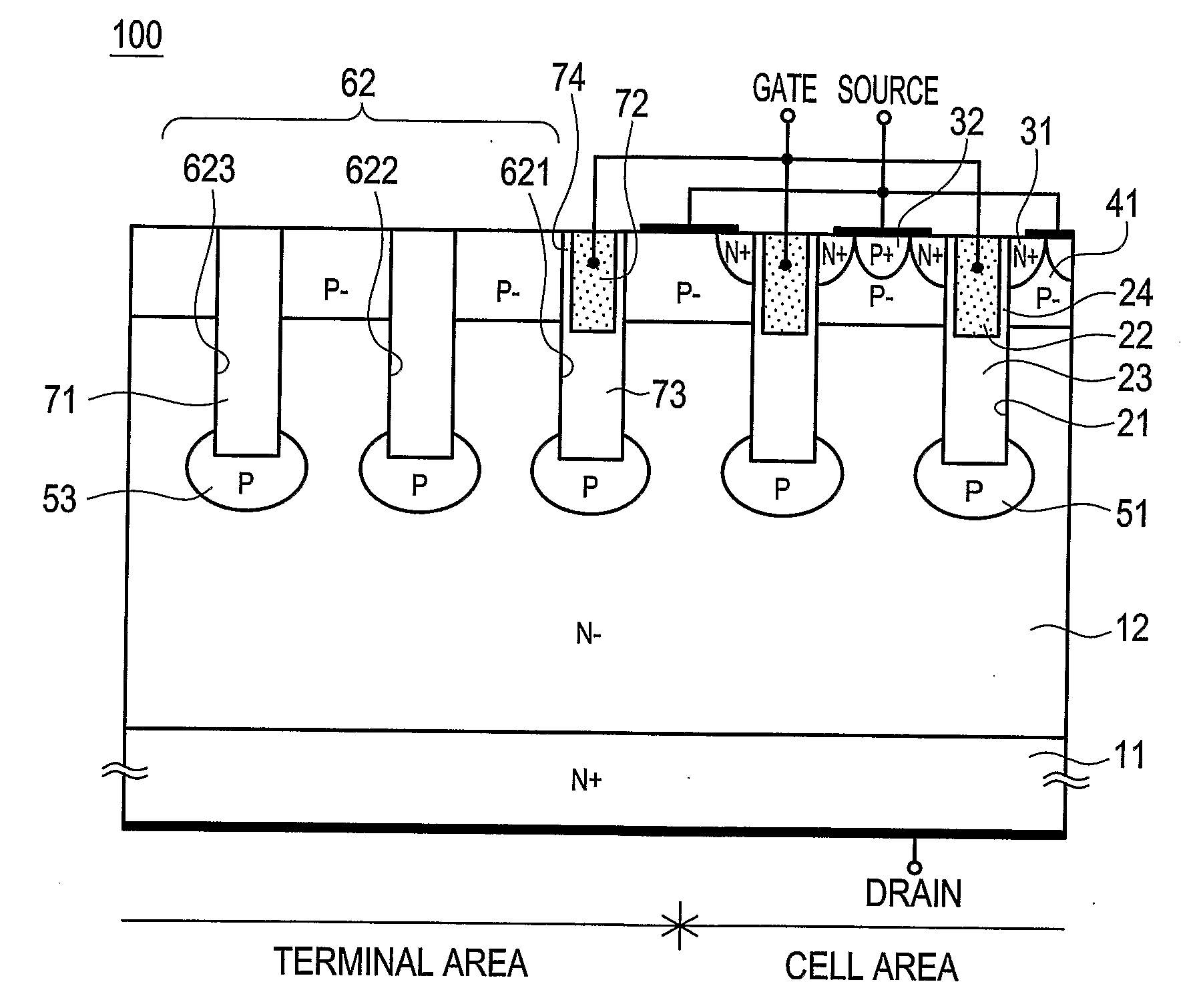
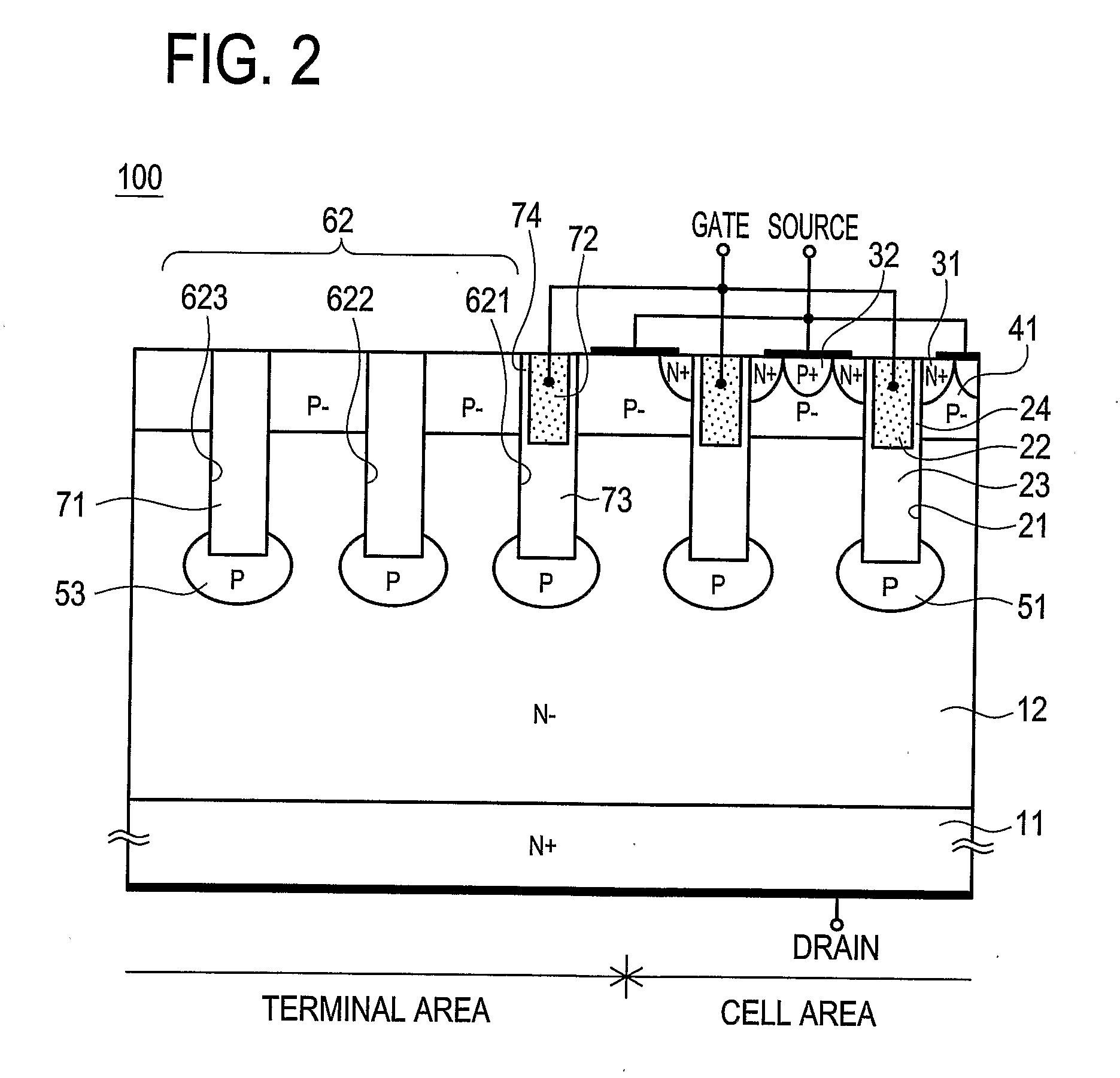
[0053]An insulated gate-type semiconductor device 100 (hereinafter referred to as “semiconductor device 100”) according to the first embodiment has such a structure as shown in the plan perspective view of FIG. 1 and the sectional view of FIG. 2. It will be noted that in the present specification, an entirety, in combination, of a starting substrate and a single crystal silicon portion formed by epitaxial growth on the starting substrate is called semiconductor substrate.

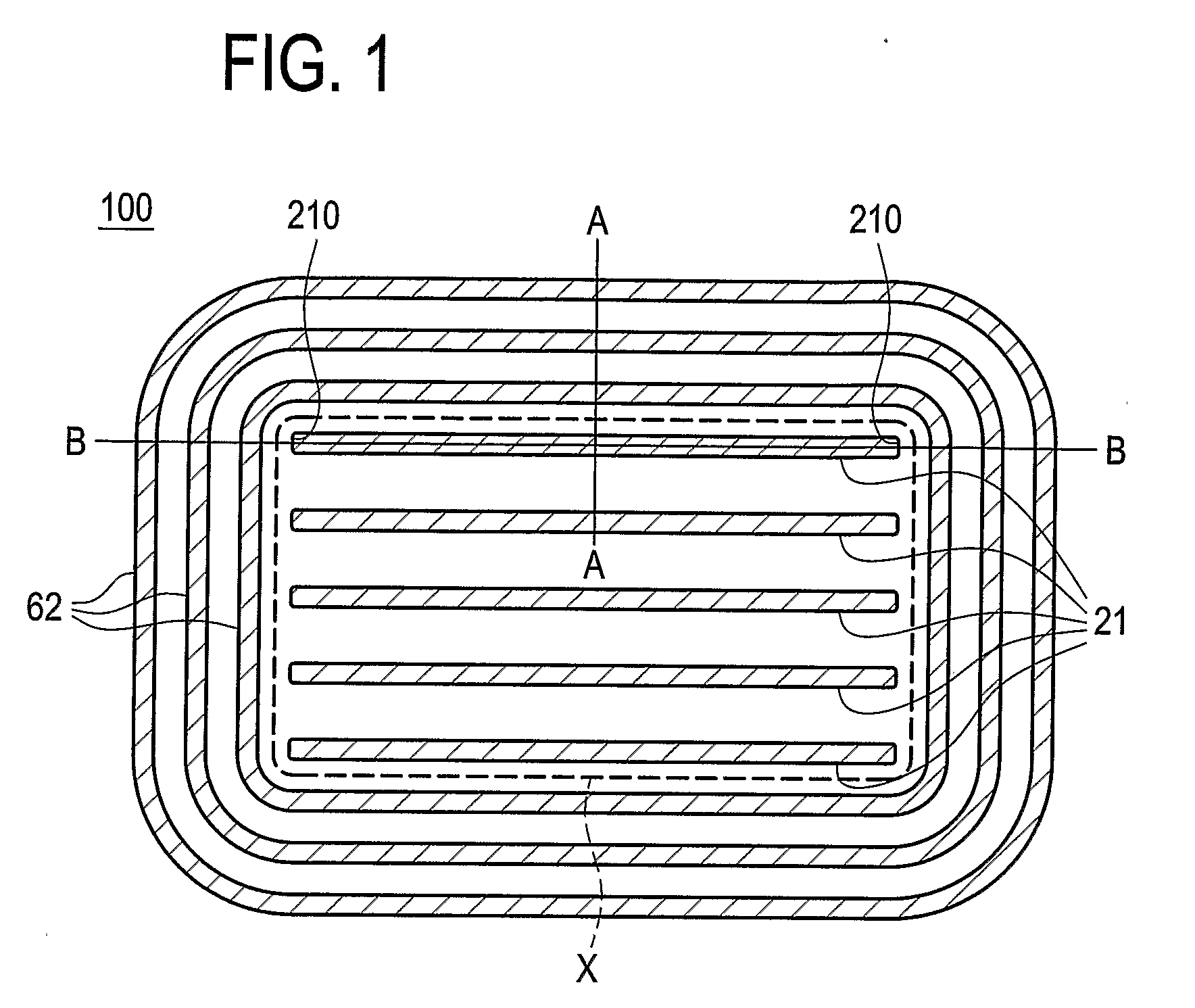
[0054]The semiconductor device 100 of this embodiment is constituted of a cell area (an area within a broken line frame x in FIG. 1) and a terminal area (an area outside of the broken line frame x in FIG. 1) surrounding the cell area. More particularly, the cell area of the semiconductor device 100 is partitioned with a terminal area. A plurality of gate trenches 21 are provided within the cell area and three terminal trenches 62 are provided within the terminal area.

[0055]Particularly, the gate trenches 21 and the ...

second embodiment

[0091]As shown in FIG. 9, a semiconductor device 200 of the second embodiment is formed with gate trenches 21 that have such a layout as to be divided into three groups in a lengthwise direction. With the semiconductor device 200, the gate trenches 21 are arranged to have a layout of being divided into a plurality of sub-trenches, so that the number of end portions 210 is larger than in the first embodiment. That is, the end portions 210 are two in number on the lengthwise direction in the first embodiment and are six in number on the lengthwise direction in this embodiment.

[0092]As shown in FIG. 10, a P−− diffusion region 52 surrounded with an N− drift region 12 is formed around the end portion 210 of individual sub-trenches. Like the first embodiment, the P−− diffusion region 52 is in connection with a P− body region 41 at an upper end thereof and also with a P diffusion region 51 at a lower end thereof. That is, the P−− diffusion region 52 serves as a supply path of holes.

[0093]T...

third embodiment

[0099]As shown in FIG. 14, a semiconductor device 300 of the third embodiment is formed with a P−− diffusion region 54 surrounded by an N− drift region 12 around one side surface of a gate trench 21. The P−− diffusion region 54 is in connection with a P− body region 41 at an upper end thereof and also with a P diffusion region 51 at a lower end, like the first embodiment. That is, the P−− diffusion region 54 serves as a hole supply path. The semiconductor device 300 of this embodiment differs from that of the first embodiment in that the hole supply path is whichever of the side surface portion and the end portion of the gate trench 21. It is to be noted that the position of the P−− diffusion region 54 may be at the side surface of the left side or the right side of the gate trench 21.

[0100]With the semiconductor device 300 of this embodiment, since the P−− diffusion region 54 serving as a hole supply path is formed on the side surface of the gate trench 21, it is easy to manufactur...


PUM


Abstract

A semiconductor 100 has a P body region and an N drift region in the order from an upper surface side thereof. A gate trench and a terminal trench passing through the P body region are formed. The respective trenches are surrounded with P diffusion regions at the bottom thereof. The gate trench builds a gate electrode therein. A P−− diffusion region, which is in contact with the end portion in a lengthwise direction of the gate trench and is lower in concentration than the P body region and the P diffusion region, is formed. The P−− diffusion region is depleted prior to the P diffusion region when the gate voltage is off. The P−− diffusion region serves as a hole supply path to the P diffusion region when the gate voltage is on.

Description

TECHNICAL FIELD[0001]The present invention relates to an insulated gate-type semiconductor device of a trench gate structure and also to a manufacturing method thereof. More particularly, the present invention relates to an insulated gate-type semiconductor with improved on-resistance characteristics, in which a drift region includes a diffusion layer of a conductive type different from that of the drift region to mitigate an electric field exerted on a drift layer.BACKGROUND ART[0002]Conventionally, trench gate-type semiconductor devices having a trench gate structure have been hitherto proposed as an insulated gate-type semiconductor device for power device applications. With this type of trench gate-type semiconductor device, high withstand voltage and low on-resistance are generally in trade-off relation.[0003]For a trench gate-type semiconductor device designed to focus attention on the above problem, the present applicant proposed an insulated gate-type semiconductor device as...

Claims


Application Information

Patent Timeline
IPC IPC(8): H01L29/78H01L21/265
CPCH01L21/26586H01L29/0623H01L29/0634H01L29/0878H01L29/7813H01L29/4238H01L29/66734H01L29/7811H01L29/42368
Inventor TAKAYA, HIDEFUMIHAMADA, KIMIMORIMIYAGI, KYOSUKE
Owner DENSO CORP
Why Eureka
Try Eureka