Electroluminescent display compensated drive signal

a technology of electric display and drive signal, applied in the field of electric display compensation drive signal, can solve the problems of increasing the electronics size of the subpixel, increasing the complexity of the subpixel, and unable to compensate for the rise or fall of vsub>oled efficiency loss, so as to reduce the aperture ratio of the subpixel, simplify the compensation of the control signal, and reduce the effect of oled efficiency loss

Active Publication Date: 2010-09-09
GLOBAL OLED TECH
View PDF26 Cites 126 Cited by
  • Summary
  • Abstract
  • Description
  • Claims
  • Application Information

AI Technical Summary

Benefits of technology

[0035]The present invention provides an effective way of providing the drive transistor control signal. It requires only one measurement of each subpixel to perform compensation. It can be applied to any active-matrix backplane. The compensation of the control signal has been simplified by using a look-up table (LUT) to change signals from nonlinear to linear so compensation can be in linear voltage domain. It compensates for Vth shift, Voled shift, and...

Problems solved by technology

Methods such as this compensate for Vth shift, but they cannot compensate for Voled rise or OLED efficiency loss.
These methods require increased subpixel complexity and increased subpixel electronics size compared to the conventional 2T1C voltage-drive subpixel circuit.
Increased subpixel complexity reduces yield, because the finer features required are more vulnerable to fabrication errors.
Particularly in typical bottom-emitting configurations, increased total size of the subpixel electronics increases power consumption because it reduces the aperture ratio, the percentage of each subpixel which emits light.
Additionally, higher currents in smaller areas increase current density in the OLED emitter, which accelerates Voled rise and OLED efficiency loss.
These methods share the disadvantages of in-pixel Vth compensation schemes, but some can additionally compensate for Voled shift or OLED efficiency loss.
However, this method requires a large number of lookup tables, consuming a significant amount of memory.
Further, this method does not recognize the problem of integrating compensation with image processing typically performed in display drive electronics.
It also does not recognize the limitations of typical display drive hardware, and so requires a timing scheme which is difficult to implement without expensive custom circuitry.
These methods cannot compensate for Voled rise or OLED efficiency loss.
Reverse-bias methods can compensate for the average Vth shift of the panel with less increase in power consumption than in-pixel compensation methods, but they require more complicated external power supplies, can require additional pixel circuitry or signal lines, and may not compensate individual subpixels that are more heavily faded than others.
However, when the drive transistors in the circuit are formed from a-Si, this assumption is not valid, as the threshold voltage of the transistors also changes with use.
The method of Arnold will thus not provide complete compensation for subpixel aging in circuits wherein transistors show aging effects.
Additio...

Method used


Image

  • Electroluminescent display compensated drive signal
  • Electroluminescent display compensated drive signal
  • Electroluminescent display compensated drive signal

Examples


first embodiment

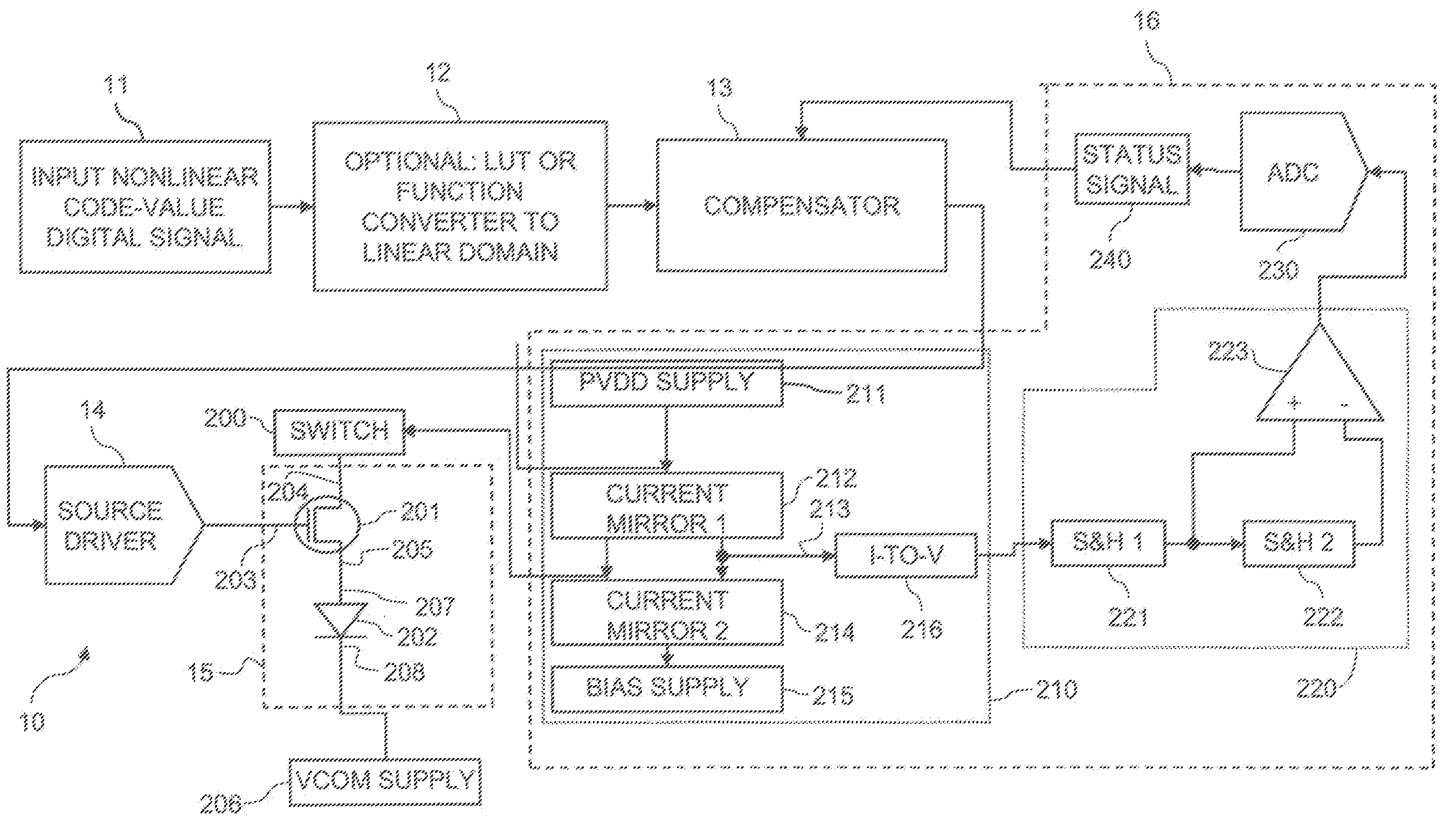
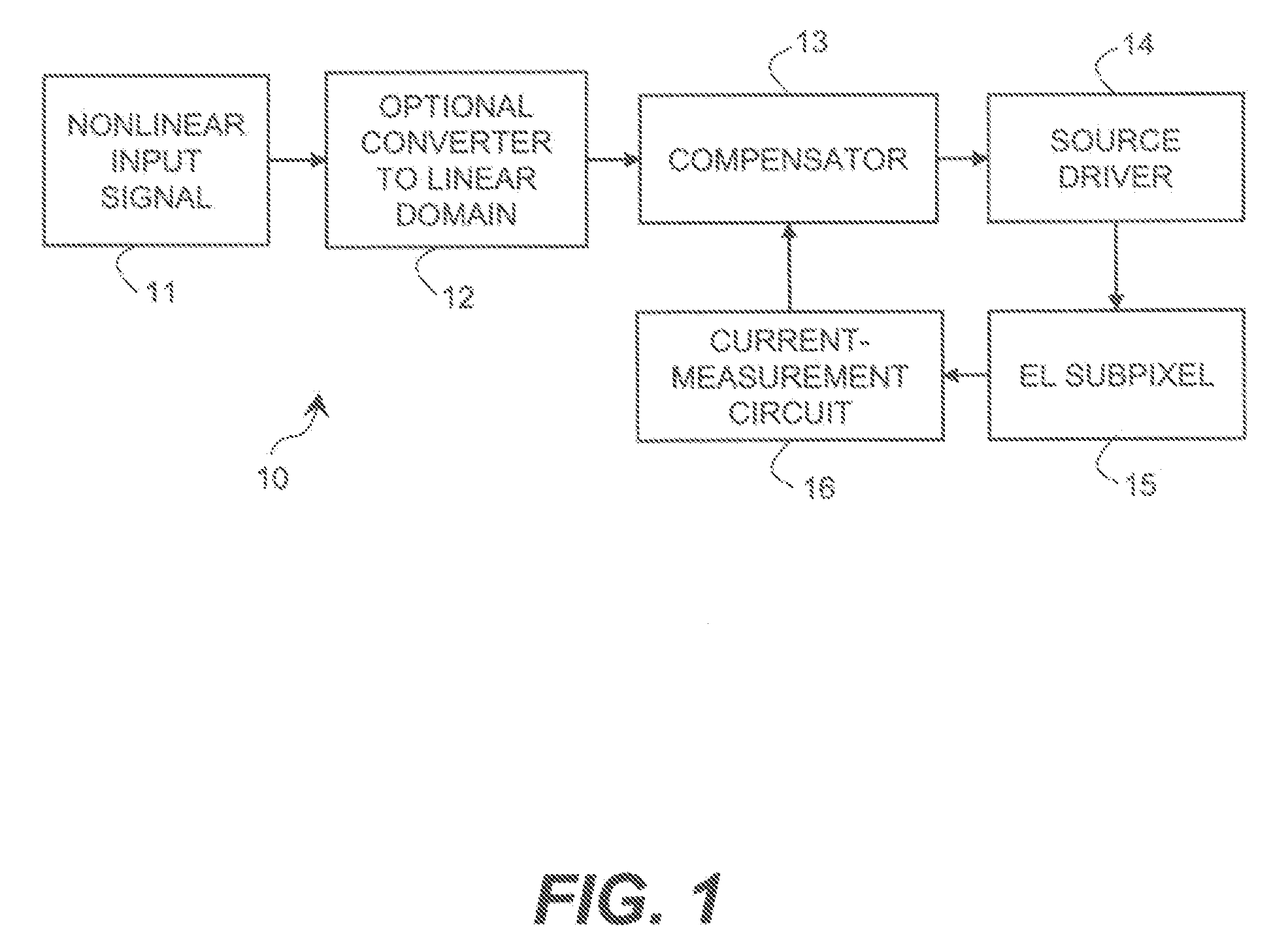
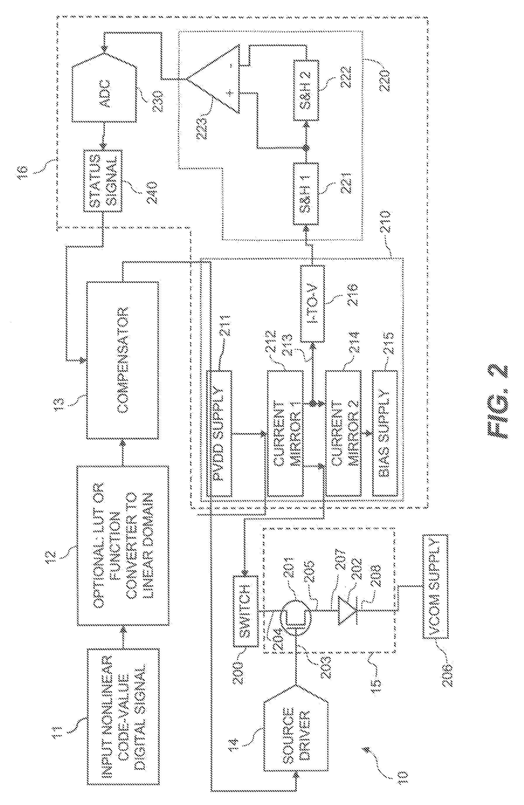
[0081]In the present invention, each current difference, e.g. 43, can be the status signal for a corresponding subpixel. For example, current difference 43 can be the status signal for the subpixel attached to row line 34b and column line 32a. In this embodiment the status signal generation unit 240 can perform a linear transform on current differences, or pass them through unmodified. All subpixels can be measured at the same measurement reference gate voltage, so that the current (43) through each subpixel at the measurement reference gate voltage meaningfully represents the characteristics of the drive transistor and EL emitter in that subpixel. The current differences 43 can be stored in memory 619.

second embodiment

[0082]In a second embodiment, memory 619 stores a respective target signal i0 611 for each EL subpixel. Memory 619 also stores a most recent current measurement i1 612 of each EL subpixel, which can be the value most recently measured by the measurement circuit for the corresponding subpixel. Measurement 612 can also be an average of a number of measurements, an exponentially-weighted moving average of measurements over time, or the result of other smoothing methods which will be obvious to those skilled in the art. Target signal i0 611 and current measurement i1 612 can be compared as described below to provide a percent current 613, which can be the status signal for the EL subpixel. The target signal for a subpixel can be a current measurement of that subpixel taken at a different time than measurement i1 612, preferably before i1, and thus percent current can represent variations in the characteristics of the respective drive transistor and EL emitter caused by operation of the ...

third embodiment

[0083]In a third embodiment, memory 619 stores a mura-compensation gain term mg 615, and a mura-compensation offset term mo 616, calculated as described below. The status signal for each EL subpixel can include a respective gain and offset, and specifically respective mg and mo values. Values mg and mo are computed with respect to a target and thus represent variations in the characteristics of the respective drive transistors and EL emitters across multiple subpixels. Additionally, any (mg, mo) pair by itself represents the characteristics of the drive transistor and EL emitter in the respective subpixel.

[0084]These three embodiments can be used together. For example, the status signal for each subpixel can include percent current, mg and mo. Compensation, described below in “Implementation,” can be performed in the same way whether the status signal indicates variations for a single subpixel over time (aging) or variations across multiple subpixels at a particular time (mura). Mem...


PUM


Abstract

Subpixels on an electroluminescent (EL) display panel, such as an organic light-emitting diode (OLED) panel, are compensated for initial nonuniformity (“mura”) and for aging effects such as threshold voltage Vth shift, EL voltage Voled shift, and OLED efficiency loss. The drive current of each subpixel is measured at one or more measurement reference gate voltages to form status signals representing the characteristics of the drive transistor and EL emitter of those subpixels. Current measurements are taken in the linear region of drive transistor operation to improve signal-to-noise ratio in systems such as modern LTPS PMOS OLED displays, which have relatively small Voled shift over their lifetimes and thus relatively small current change due to channel-length modulation. Various sources of noise are also suppressed to further increase signal-to-noise ratio.

Description

CROSS REFERENCE TO RELATED APPLICATIONS[0001]Reference is made to commonly-assigned, co-pending U.S. patent application Ser. No. 11 / 962,182 filed Dec. 21, 2007, entitled “Electroluminescent Display Compensated Analog Transistor Drive Signal” to Leon et al, U.S. patent application Ser. No. 12 / 274,554 filed Nov. 20, 2008, entitled “Electroluminescent Display Initial-Nonuniformity-Compensated Drive Signal” to Leon et al. and U.S. patent application Ser. No. ______ filed ______, entitled “Electroluminescent Subpixel Compensated Drive Signal” by Levey et al, the disclosures of which are incorporated herein.FIELD OF THE INVENTION[0002]The present invention relates to control of a signal applied to a drive transistor for supplying current through a plurality of electroluminescent emitters on an electroluminescent display.BACKGROUND OF THE INVENTION[0003]Flat-panel displays are of great interest as information displays for computing, entertainment, and communications. For example, electrolu...

Claims


Application Information

Patent Timeline
IPC IPC(8): G09G5/00
CPCG09G3/3208G09G2320/0233G09G2320/0285G09G2360/16G09G2320/043G09G2320/045G09G2320/0693G09G2320/029G09G2340/10G09G3/30
Inventor LEVEY, CHARLES I.HAMER, JOHN W.
Owner GLOBAL OLED TECH
Why Eureka
Try Eureka