

Optical semiconductor device, socket, and optical semiconductor unit
- Summary
- Abstract
- Description
- Claims
- Application Information
AI Technical Summary
Benefits of technology
Problems solved by technology
Method used
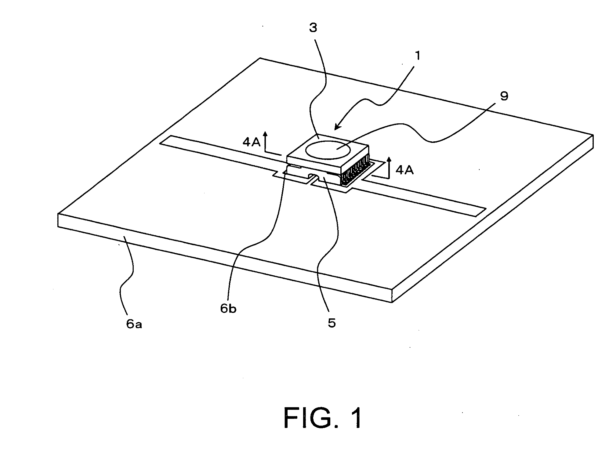
Image

Examples
example 1
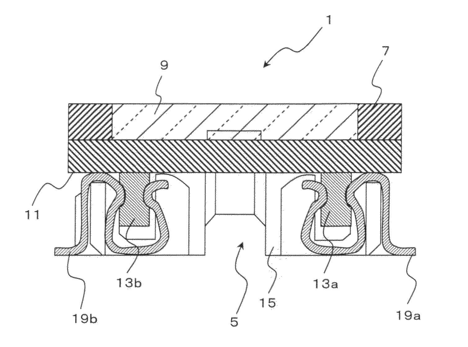
[0115]According to the design method using the finite element method described in the first embodiment, volumes of the main body 7 and the electrode portions 13a and 13b of the LED device 3 were calculated so as to optimize the thermal property data.
[0116]The LED 9 had a size of 1 mm square and a height of 0.1 mm. A thermal conductivity of the LED 9 and an input power supplied to the LED 9 were 42 W / mK and 1 W (at a room temperature), respectively.
[0117]A junction temperature of the LED 9 was 200° C. and the substrate 6a was a glass-epoxy substrate (FR-4) having a size of 50 mm square and a thickness of 0.8 mm.
[0118]As a material of the main body 7, Al2O3 (having a thermal conductivity of 18 W / mK) was used. As a material of the electrode portions 13a and 13b, oxygen-free copper (having a thermal conductivity of 390 W / mK) was used. Then, a relationship between a volume of the main body 7 and a temperature of the LED 9 and a relationship between a volume of the electrode portions 13a ...
example 2
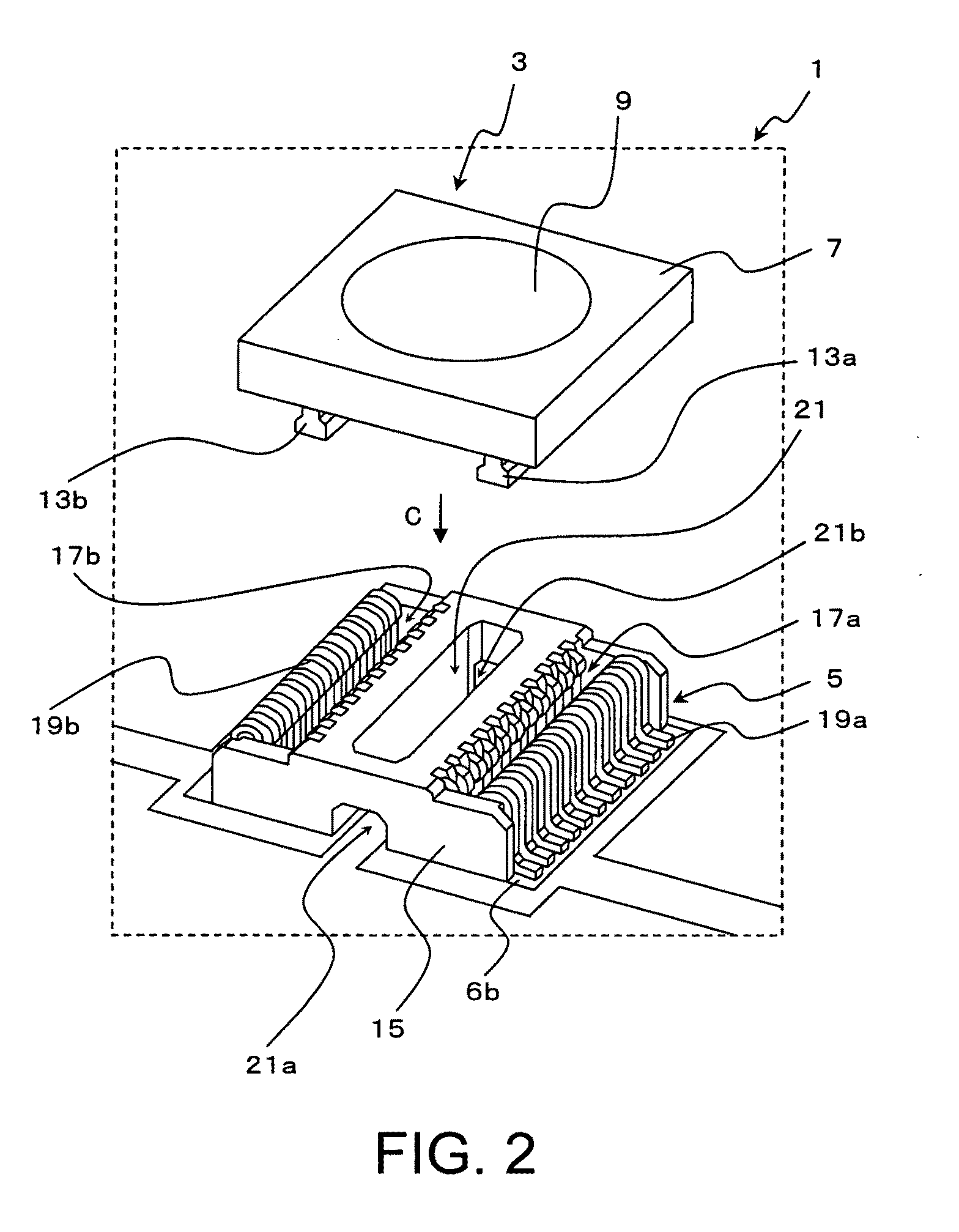
[0122]According to the design method using the finite element method described in the first embodiment, comparison was made between junction temperatures of the LED 9 when the socket 5 according to the first embodiment was used and when the socket 5a according to the fourth embodiment was used.
[0123]Specifically, each of the eleven socket terminals 19a and the eleven socket terminals 19b of the socket 5 had a width of 0.2 mm and these socket terminals were disposed at a distance of 0.2 mm from one another. On the other hand, each of the four socket terminals 43a and the four socket terminals 43b of the socket 5a had a width of 0.91 mm and these socket terminals were disposed at a distance of 0.2 mm from one another. For all of those socket terminals, a contact length in a direction perpendicular to a width direction of each socket terminal was 0.92 mm.
[0124]As a material of the socket terminal, phosphor bronze (having a thermal conductivity of 63 W / mK) and a copper alloy (having a t...
PUM
 Abstract
Description
Claims
Application Information