Semiconductor device for signal amplification

a technology of signal amplification and semiconductor devices, which is applied in the direction of amplifier combinations, amplifiers with field-effect devices, gain control, etc., can solve the problems of poor power efficiency, large consumption current, and deterioration of gain controllability, so as to achieve fine resolution, reduce consumption current, and make the dynamic range high

Active Publication Date: 2010-09-16
RENESAS ELECTRONICS CORP
View PDF6 Cites 17 Cited by
  • Summary
  • Abstract
  • Description
  • Claims
  • Application Information

AI Technical Summary

Benefits of technology

[0015]Voltage levels of each node of the ladder network are different; correspondingly, voltage levels supplied to each of the first transconductance stages are different. The output signal line is provided common to the first transconductance stages. The present first transconductance stages are selectively enabled according to the control word. It is possible to set the current step which appears in the output signal line to any value, leading to realization of gain of fine resolution. It is also possible to make the dynamic range high by increasing the number of the first transconductance stages. The number of the first transconductance stages enabled at the same time is reduced, and the consumption current can be reduced.

Problems solved by technology

However, according to the configuration of Patent Document 1, when all control word bits C(0)-C(N−1) are “1” (H level), all the transconductance amplifiers flow current via the output load; therefore, the consumption current becomes very large.
Therefore, there arises a problem that power efficiency is poor and gain controllability deteriorates at the time of generating a high output voltage.

Method used


Image

  • Semiconductor device for signal amplification
  • Semiconductor device for signal amplification
  • Semiconductor device for signal amplification

Examples


embodiment 1

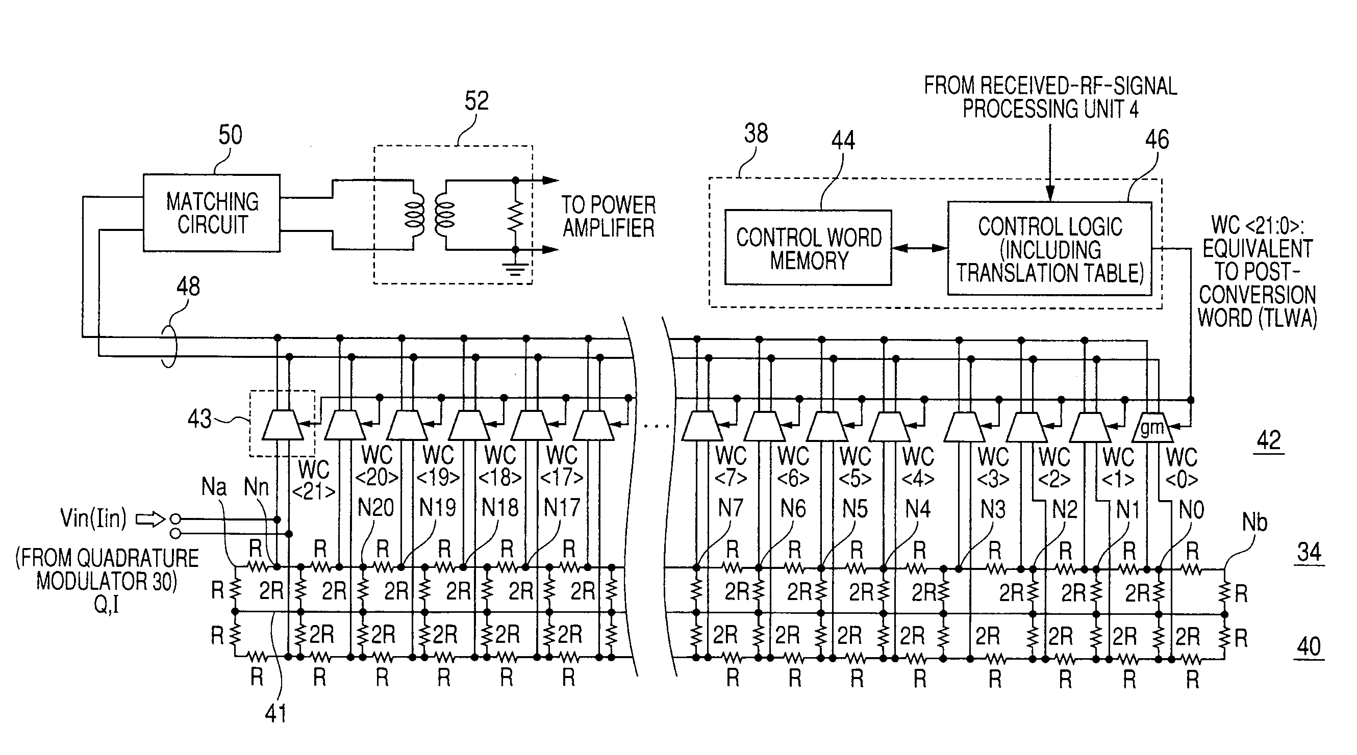
[0053]FIG. 1 illustrates schematically an entire configuration of a mobile terminal including a semiconductor device for signal amplification according to Embodiment 1 of the present invention. In FIG. 1, the mobile terminal includes a reception path RX which receives and reproduces a signal supplied via an antenna 1, a transmitting path TX which transmits a signal / data via the antenna 1, and a transmitting / receiving duplex circuit 2 which couples the transmitting path TX and the reception path RX to the antenna 1. The present mobile terminal performs communication according to UMTS, employs an FDD system as the communications system, and performs transmission and reception in parallel on a full-duplex transmission system, by allocating different frequency bands to transmission and reception. The transmitting / receiving duplex circuit 2 performs transmission and reception in parallel to the antenna 1 using different frequency bands.

[0054]The transmitting / receiving duplex circuit 2 in...

embodiment 2

[0110]FIG. 8 illustrates a model of a delay circuit of the transconductance amplifier stage 43 and the R-2R ladder network. In FIG. 8, the configuration of three transconductance amplifier stages 43 and an R-2R ladder network which has the corresponding nodes is illustrated as an example. In the configuration illustrated in FIG. 8, a resistor R and a parasitic capacitance Cp are coupled to each of both inputs of the transconductance amplifier stage 43. Therefore, when voltage of the input signal is sequentially transmitted via a resistance element R of the R-2R ladder network, propagation delay of a signal occurs. When such propagation delay of the input signal occurs, phase fluctuation of a signal may occur in switching the transconductance amplifier stages.

[0111]FIG. 9 illustrates waveforms of the result that the source signal and the delayed signal are combined (added) in the delay model illustrated in FIG. 8. The voltage gain in the delay circuit is set to one. In FIG. 9, the ho...

embodiment 3

[0128]FIG. 12 illustrates schematically a configuration of a variable gain driver according to Embodiment 3 of the present invention. In FIG. 12, the variable gain driver 34 is different in configuration from the variable gain driver illustrated in FIG. 11 in the following points. That is, transconductance amplifiers 80, 81, and 82 of which the transconductance gm is enlarged every two times are provided in parallel with the input node Nn. The transconductance amplifier 80 has two times greater current supply capability than that of the transconductance amplifier stage 43, and is formed equivalently by two transconductance amplifier stages 43 coupled in parallel. The transconductance amplifier 81 has four times greater current supply capability than that of the transconductance amplifier stage 43, and is formed equivalently by four transconductance amplifier stages 43 coupled in parallel. The transconductance amplifier 82 has eight times greater current supply capability than that o...


PUM


Abstract

A semiconductor device for transmitting-signal amplification which has a fine resolution, a high dynamic range, a small occupied area, and low power consumption, is realized. An input signal amplitude is reduced every one half by a ladder network, and a transconductance amplifier stage is arranged corresponding to each node of the ladder network. An output of the transconductance amplifier stage is coupled to an output signal line in common. According to a control word WC<21:0>, the transconductance amplifier stage is enabled selectively, and the output current which appears in the output signal line is added.

Description

CROSS REFERENCES TO RELATED APPLICATIONS[0001]The disclosure of Japanese Patent Application No. 2009-59951 filed on Mar. 12, 2009 including the specification, and drawings and abstract is incorporated herein by reference in its entirety.BACKGROUND OF THE INVENTION[0002]The present invention relates to a semiconductor device for signal amplification, in particular, relates to a configuration of a transmission amplifying device for controlling gain of a transmitting signal of a transmitting section in mobile communications equipment.[0003]As a communications system to a mobile terminal etc. in a mobile communications field, there is currently UMTS (Universal Mobile Telecommunications System; European standard communications system: compatible with W-CDMA in Japan). UMTS has spread widely as a communications system of a third-generation digital mobile-phone.[0004]In the UMTS transmission system, a power control range is 86 dB and a high dynamic range is required. In order to respond to...

Claims


Application Information

Patent Timeline
Patent Type & Authority Applications(United States)
IPC IPC(8): H03F3/68
CPCH03F1/301H03G3/3042H03F3/245H03F3/45179H03F2200/222H03F2200/336H03F2200/447H03F2200/451H03F2200/456H03F2200/534H03F2203/45544H03F2203/45604H03F2203/45616H03F2203/45728H03G1/0088H03F3/195
Inventor MIZOKAMI, MASAKAZUMARUYAMA, TAKAYAHORI, KAZUAKI
Owner RENESAS ELECTRONICS CORP
Why Eureka
Try Eureka