Control signal transmitting system of a semiconductor device

a technology of control signal and transmitting system, which is applied in the direction of information storage, static storage, digital storage, etc., can solve the problems of relatively large amount of power consumed to transmit clock based signals, large capacity loading of capacitors, etc., and achieve the effect of reducing the amount of power consumed charging and reducing the power consumption of control signal transmission

Inactive Publication Date: 2010-09-16
SAMSUNG ELECTRONICS CO LTD
View PDF7 Cites 26 Cited by
  • Summary
  • Abstract
  • Description
  • Claims
  • Application Information

AI Technical Summary

Benefits of technology

[0011]Exemplary embodiments of the invention provide a control signal transmitting system of a semiconductor device capable of reducing the power consumption of control signal transmission in a semiconductor memory device. The control signal transmitting system shown in FIG. 7 reduces the amount of power consumed charging and discharging the bus line L10 when the clock-based (periodic) control signals are transmitted.

Problems solved by technology

Therefore, capacitative line loading is relatively large.
Therefore, a relatively large amount of power is consumed to transmit the clock based signals.

Method used


Image

  • Control signal transmitting system of a semiconductor device
  • Control signal transmitting system of a semiconductor device
  • Control signal transmitting system of a semiconductor device

Examples


Embodiment Construction

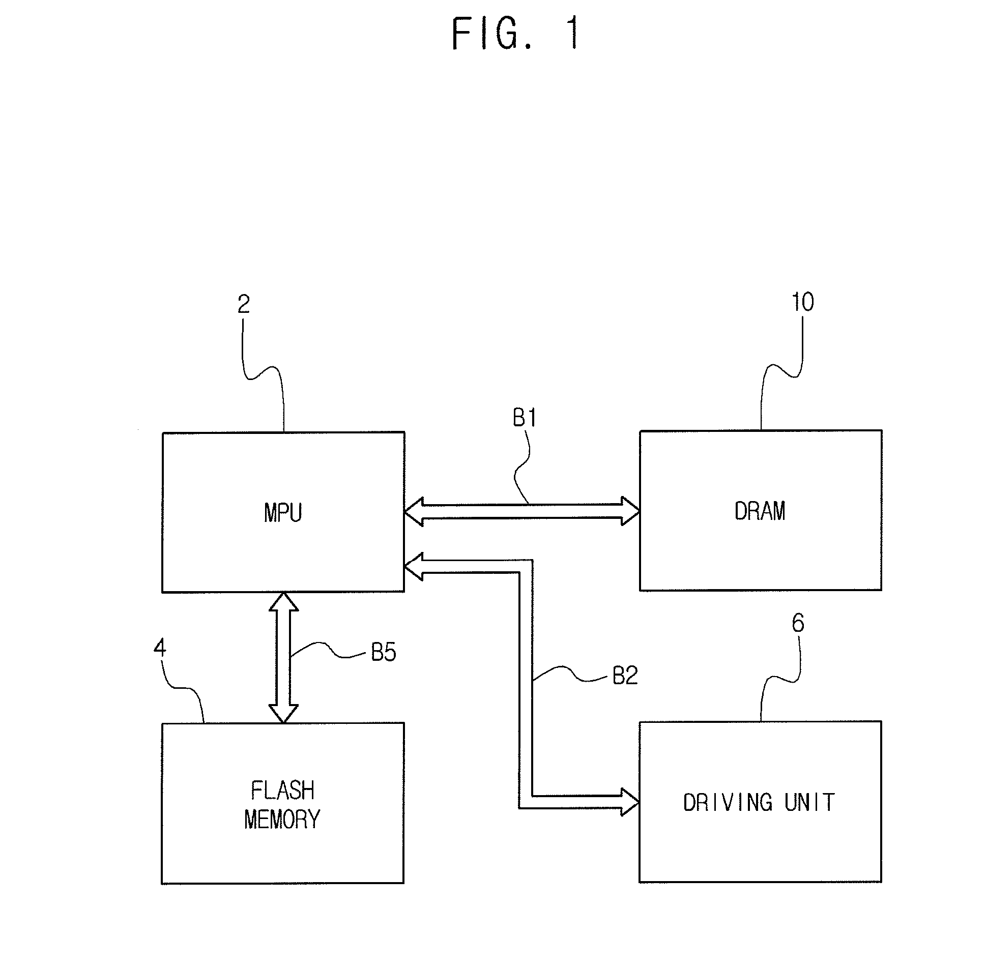
[0041]FIG. 1 is a block diagram of a related art data processing system that can be improved by incorporating the control signal transmitting system of FIG. 7 within the DRAM 10 according to an exemplary embodiment of the invention. The DRAM 10 in the data processing system of FIG. 1 will consume less power if it incorporates the control signal transmitting system of FIG. 7.

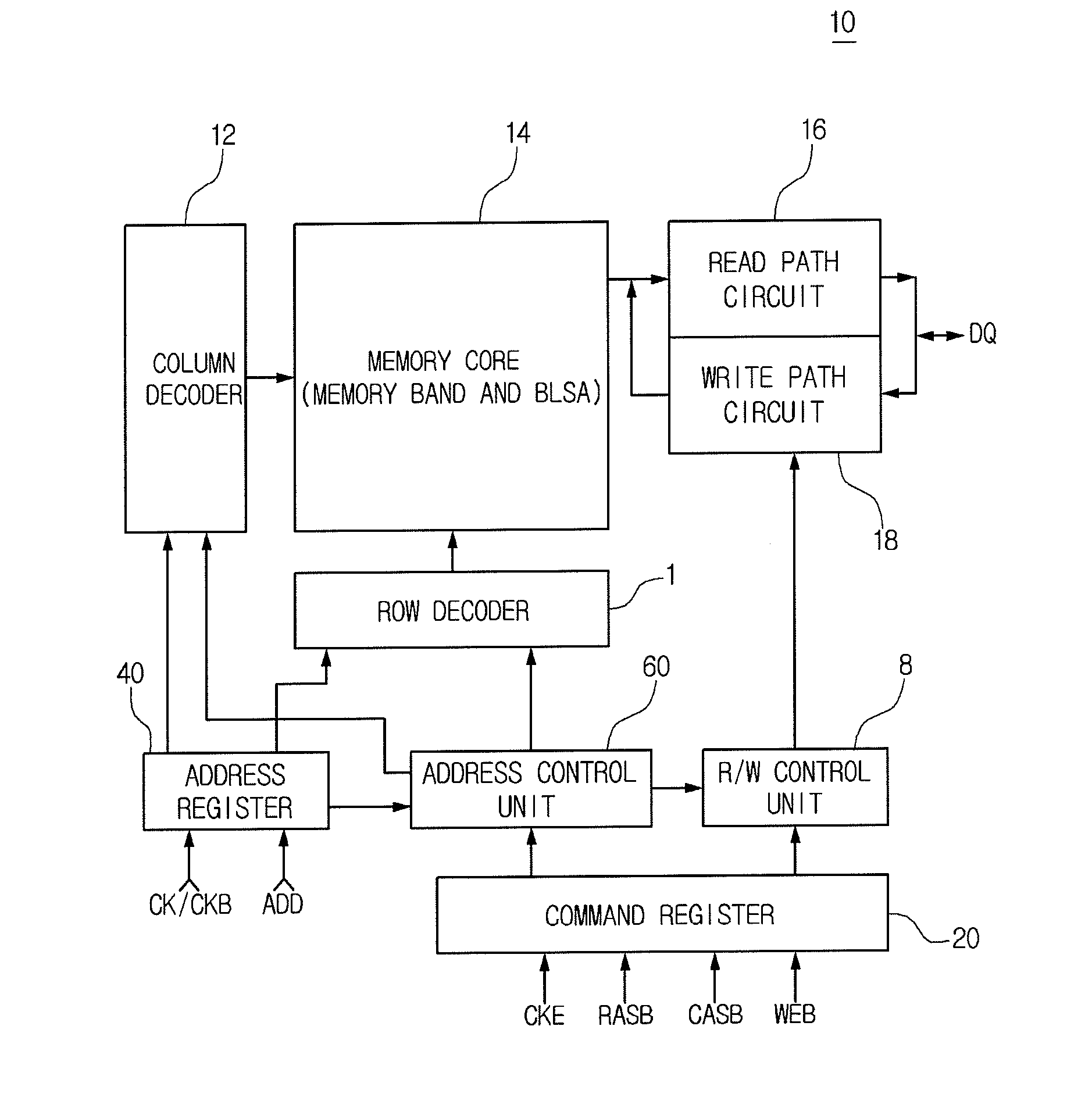
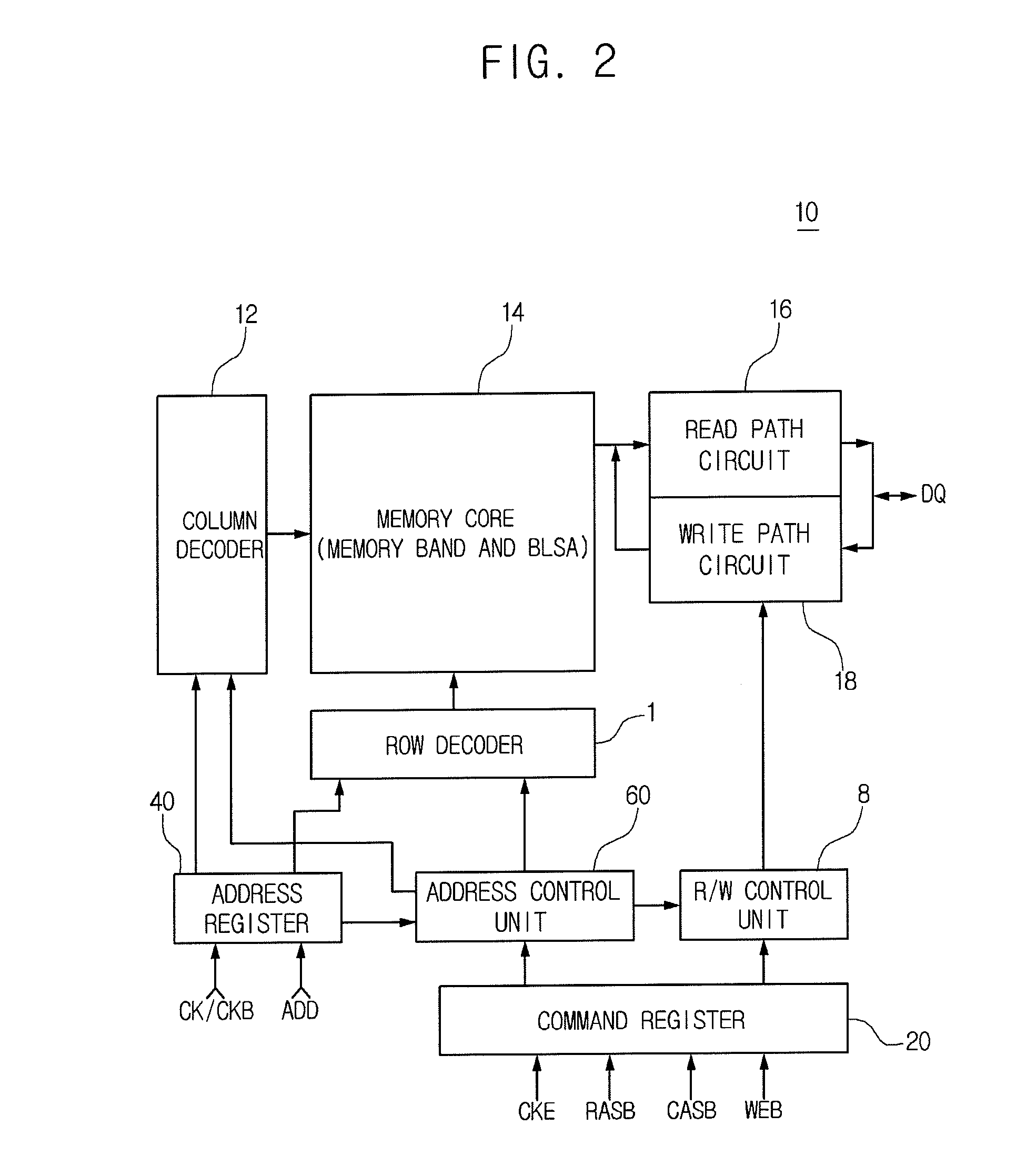
[0042]FIG. 2 is a block diagram of the DRAM shown in FIG. 1. FIG. 3 is a diagram illustrating an example of the read path circuit 16 shown in FIG. 2. FIG. 4 is a layout diagram of a DRAM chip implementing the DRAM 10 in FIG. 1. FIG. 4 illustrates a transmission path of a control signal shown in FIG. 3. FIG. 5 is a diagram illustrating the connection of a bus line provided in the transmission path shown in FIG. 4. FIG. 6 is a timing diagram of the input / output signals of the transmission path in FIG. 5.

[0043]FIG. 2 is a block diagram of the DRAM 10 illustrating the wiring relationship among general functional bloc...


PUM


Abstract

Exemplary embodiments relate to a control signal driving device of a semiconductor device, including: a bus line; a converter receiving a first periodic control signal having the period (frequency) of a clock signal, converting the first periodic control signal into a converted control signal that has twice the period (half the frequency) of the clock signal, and outputting the converted control signal to the bus line; and a restoring unit connected to the opposite end of the bus line and receiving the converted control signal and restoring the converted control signal back into the first periodic control signal.

Description

CROSS-REFERENCE TO RELATED APPLICATIONS[0001]This U.S. non-provisional patent application claims the benefit, under 35 U.S.C. §119, of Korean Patent Application 10-2009-0021068, filed on Mar. 12, 2009, in the Korean Intellectual Property Office, the entire contents of which are incorporated by reference herein.BACKGROUND[0002]1. Field of the Invention[0003]Exemplary embodiments of the present invention relate to a semiconductor device, and more particularly, to a control signal driving device of a semiconductor memory device.[0004]2. Description of the Related Art[0005]In recent years, the speed and the degree of miniaturization of semiconductor memory devices, such as dynamic random access memories (DRAMS), have increased continuously to meet consumer demands. DRAMs store information in arrays of memory cells that include capacitors formed in integrated circuits on a chip. The DRAM devices having one access transistor and one storage capacitor in each memory cell are generally used...

Claims


Application Information

Patent Timeline
Patent Type & Authority Applications(United States)
IPC IPC(8): G11C11/24G11C7/00G11C8/18
CPCG11C7/1048G11C7/1051G11C7/1069G11C11/4096G11C7/222G11C11/4076G11C11/4091G11C7/22G11C11/4093
Inventor HWANG, HYONG-RYOLOH, CHI-SUNGKANG, SANG-KYU
Owner SAMSUNG ELECTRONICS CO LTD
Why Eureka
Try Eureka