Semiconductor integrated circuit device

a technology of integrated circuit devices and semiconductors, applied in static storage, digital storage, instruments, etc., to achieve the effect of improving the reliability reducing the number of times of disturbance, and reducing the size of semiconductor integrated circuit devices

Active Publication Date: 2010-09-16
RENESAS ELECTRONICS CORP
View PDF5 Cites 7 Cited by
  • Summary
  • Abstract
  • Description
  • Claims
  • Application Information

AI Technical Summary

Benefits of technology

[0028](1) The number of circuits of MG driver circuits and CG drivers can be reduced and the number of times of disturb occurrence can be decreased, while avoiding an increase in the chip area.
[0029](2) In consequence of the above advantage mentioned in (1), it is possible to improve the reliability of a semiconductor integrated circuit device, while decreasing its size.

Problems solved by technology

However, the inventors found that the above-mentioned technique as a countermeasure against the disturb experienced by a nonvolatile memory has problems discussed below.

Method used


Image

  • Semiconductor integrated circuit device
  • Semiconductor integrated circuit device
  • Semiconductor integrated circuit device

Examples


first embodiment

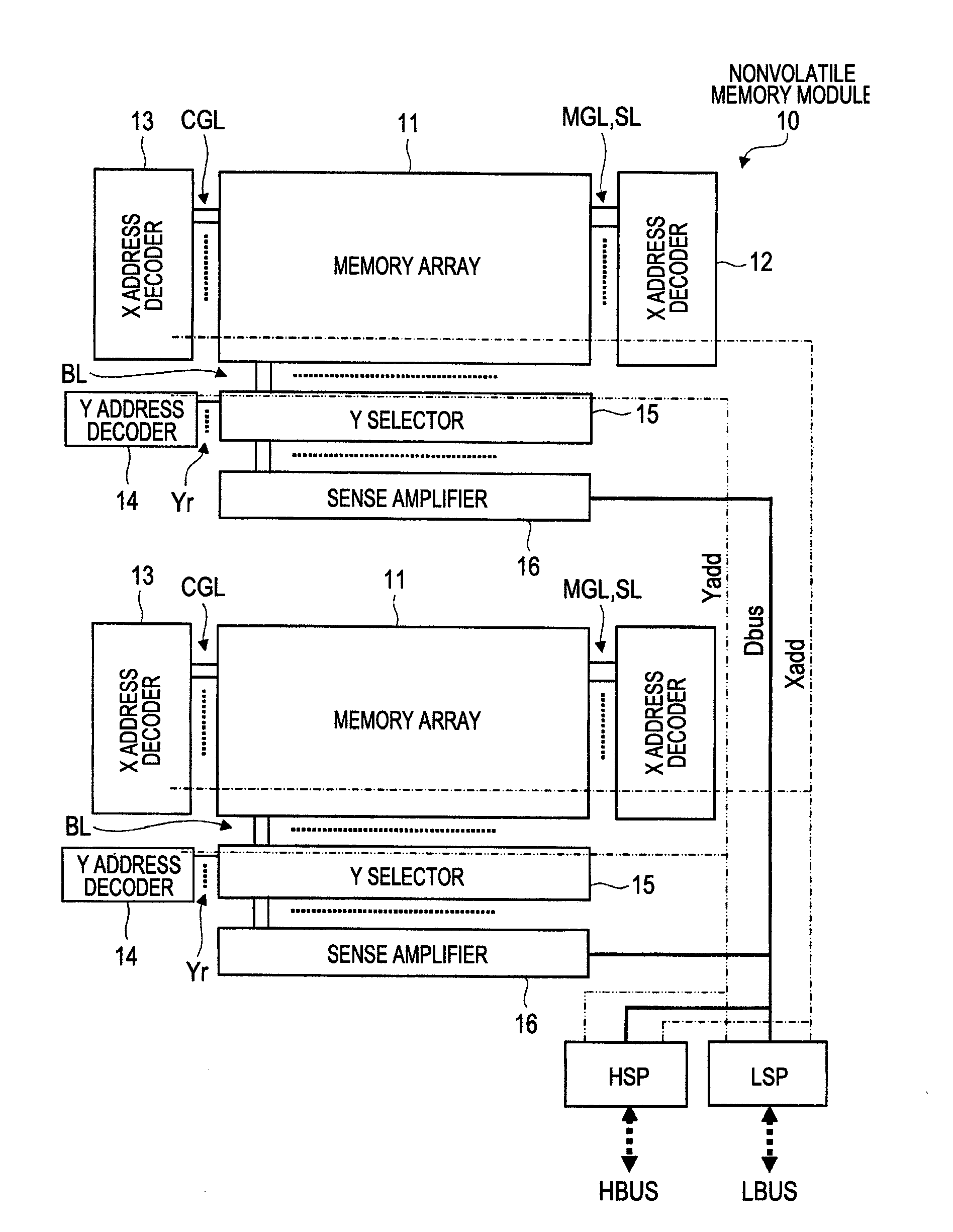
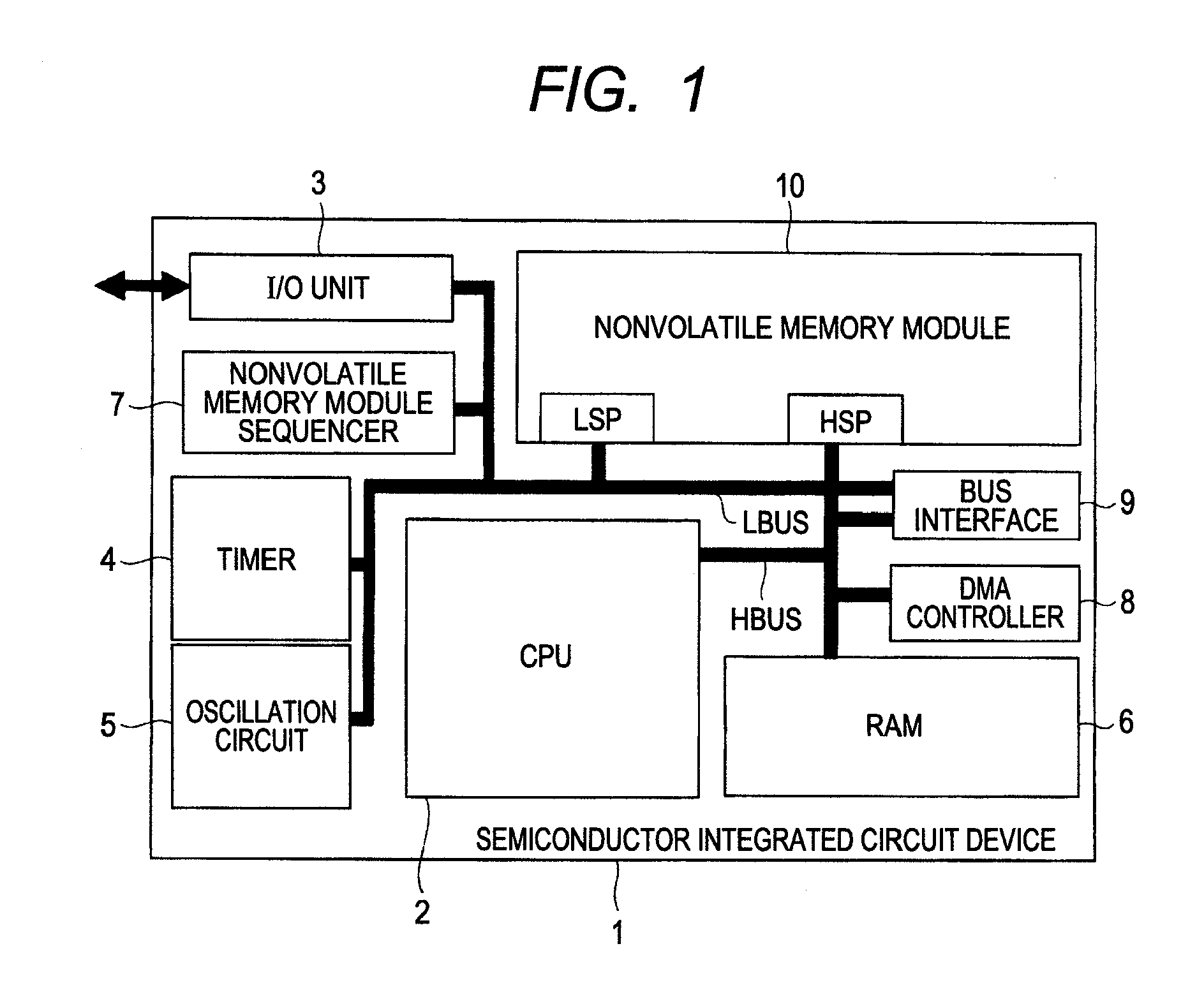
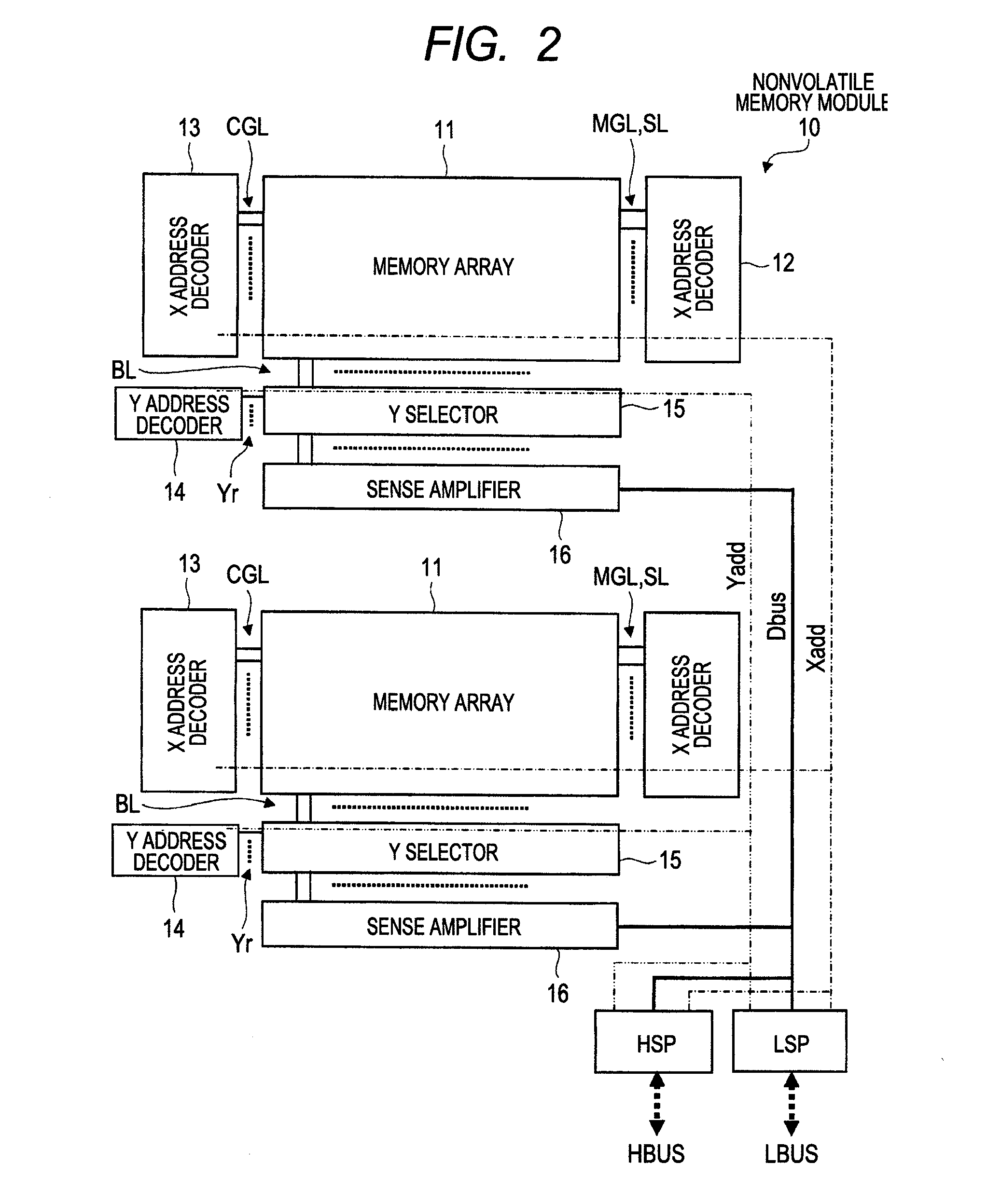
[0051]FIG. 1 is a block diagram showing a configuration example of a semiconductor integrated circuit device according to a first embodiment of the present invention. FIG. 2 is an illustrative diagram showing a configuration example of a nonvolatile memory module provided in the semiconductor integrated circuit device of FIG. 1. FIG. 3 is an illustrative diagram showing a configuration example of a memory cell provided in the nonvolatile memory module of FIG. 2. FIG. 4 is an explanatory table listing voltage conditions for write, erase, and read in the memory cell of FIG. 3. FIG. 5 is an illustrative diagram showing a configuration example of a memory array shown in FIG. 2. FIG. 6 is a timing chart showing operating waveforms of signals representing an example of write operation in a memory array of FIG. 18. FIG. 7 is a timing chart representing an example of write operation in the memory array of FIG. 5. FIG. 8 is a timing chart showing operating waveforms of signals in erase opera...

second embodiment

[0111]FIG. 13 is an illustrative diagram showing a configuration example of a memory array according to a second embodiment of the present invention. FIG. 14 is an illustrative diagram showing another configuration example of the memory array of FIG. 13.

[0112]In the second embodiment, FIG. 13 shows an example of modification to the first embodiment, wherein the elements of the MG buffer circuits 21 shown in FIG. 5 are replaced by switch transistors.

[0113]The MG buffer circuits 21 shown in FIG. 5 for the preceding first embodiment are, for example, of a CMOS type which comprises a p-conducting (P-type) MOSFET and an n-conducting (N-type) MOSFET which are not shown. However, in FIG. 13 for the second embodiment, the components of the MG buffer circuits 21 are replaced by switch transistors SWs and these transistors SWs (e.g., N-type MOSFETs) are on / off controlled by a control signal MGT. Therefore, a control signal MGDN is only supplied to the MG buffer circuits 21.

[0114]FIG. 14 shows...

third embodiment

[0119]FIG. 15 is a set of graphs to explain an example of threshold voltage control for memory cells according to a general method of storing one unit of data per cell. FIG. 16 is a set of graphs to explain an example of threshold voltage control for memory cells provided in a memory array according to a third embodiment of the present invention. FIG. 17 is an illustrative diagram showing a configuration example of a memory array according to the third embodiment of the present invention.

[0120]In the third embodiment, a complementary storage method that stores one unit of data using two memory cells is applied to the memory array configuration described in the preceding first embodiment.

[0121]Here, the complementary storage method is explained.

[0122]In the general method of storing one unit of data using one memory cell (storing one unit of data per cell), the threshold voltage for the transistors constituting each memory cell is controlled so that the threshold voltage in a data wr...


PUM


Abstract

This invention is to reduce the number of memory gate drivers, while lessening the number of times of disturb occurrence in a memory array configuration that implements writing in small byte units. A memory array comprises a plurality of sub-arrays, MG transfers, SL drivers, and CG drivers. Each sub-array includes a plurality of memory gate lines, control gate lines, source lines, and bit lines. Memory cells are arranged in positions of intersections of these lines. The control gate lines, CG drivers, source lines, and SL drivers are common to the sub-arrays, whereas the memory gate lines and MG buffer circuits are provided for each sub-array. Thereby, the units in which data is written are decreased and adverse effects of disturb are reduced without increasing the circuit size of the memory array.

Description

CROSS-REFERENCE TO RELATED APPLICATIONS[0001]The disclosure of Japanese Patent Application No. 2009-58894 filed on Mar. 12, 2009 including the specification, drawings and abstract is incorporated herein by reference in its entirety.BACKGROUND OF THE INVENTION[0002]The present invention relates to a technique for improving the reliability of a nonvolatile memory module and, particularly, to a technique that is effective for preventing data corruption due to disturb encountered in writing in small byte units.[0003]In recent years, for semiconductor integrated circuit devices such as microcomputers incorporating a nonvolatile memory and microcomputers of a so-called flash memory built-in type, there is a need to mount a flash memory module that supports writing in small byte units.[0004]FIG. 18 is an illustrative diagram showing a configuration example of a memory array 100 provided in a flash memory module examined by the present inventors.[0005]In the memory array 100, as shown, SL d...

Claims


Application Information

Patent Timeline
Patent Type & Authority Applications(United States)
IPC IPC(8): G11C16/06G11C7/10
CPCG11C7/02G11C16/3418G11C16/32G11C16/06
Inventor MATSUBARA, KENKASAI, HIDEOKAWADA, KENJIMIZUNO, MAKOTO
Owner RENESAS ELECTRONICS CORP
Why Eureka
Try Eureka