Optical transmitter device and optical transmitter module

a technology of optical transmitter and optical module, which is applied in the direction of electromagnetic transceivers, semiconductor lasers, printed circuit aspects, etc., can solve the problems of inessential power consumption, optical module hindering size reduction, and unable to achieve favorable waveforms by driving only the electro-absorption optical modulator devices alone. achieve excellent optical transmission waveform quality and reduce the size of the optical transmitter modul

Active Publication Date: 2010-09-16
LUMENTUM JAPAN INC
View PDF28 Cites 21 Cited by
  • Summary
  • Abstract
  • Description
  • Claims
  • Application Information

AI Technical Summary

Benefits of technology

[0009]The present invention has been made in view of the problems described above, and it is therefore an object of the present invention to provide an optical transmitter device and an optical transmitter module that are capable of reducing the optical transmitter module size while maintaining a state where an excellent optical transmission waveform quality is obtained over a wide range of frequencies.
[0012]According to the present invention, flat impedance characteristics are obtained over a wide range of frequencies from the lower cutoff frequency of the first termination resistor circuit to the upper cutoff frequency of the second termination resistor circuit. An excellent optical transmission waveform quality is therefore obtained over a wide range of frequencies. Further, with the second termination resistor circuit provided in the printed circuit board, the optical transmitter module can have a smaller size than that in prior art. The present invention can thus make an optical transmitter module small in size while maintaining a state where an excellent optical transmission waveform quality is obtained over a wide range of frequencies.
[0013]According to one aspect of the present invention, the optical transmitter device further includes a transmission line that electrically connects the optical transmitter module and the printed circuit board, in which: the impedance of the first termination resistor circuit in the pass frequency band thereof corresponds to a characteristic impedance of the transmission line; and the impedance of the second termination resistor circuit in the pass frequency band thereof corresponds to the characteristic impedance of the transmission line. According to the one aspect of the present invention, signal attenuation due to electrical return loss may be reduced.
[0014]Further, according to another aspect of the present invention, the optical transmitter device is provided in which a signal output from the signal output circuit has a given value or less as a difference between an amplitude at a junction where the first termination resistor circuit connects with the transmission line and an amplitude at a junction where the second termination resistor circuit connects with the transmission line. According to the another aspect of the present invention, a better optical transmission waveform quality may be obtained more easily than when an optical transmitter device is structured otherwise.

Problems solved by technology

Obtaining a favorable waveform by merely driving the electro-absorption optical modulator device alone is therefore difficult due to an impedance inconsistency.
However, in this type of optical modules having the termination circuit structure described above, the need to apply a bias voltage to the electro-absorption optical modulator device causes an originally unnecessary direct current in the resistor device, which can lead to inessential power consumption.
However, as optical transceivers become smaller in size in accordance with a standard called Multi Source Agreement (MSA), a problem has arisen in that the use of the conventional technology described above in building an optical module hinders size reduction.
Manufacturing a small-sized optical module with this technology is therefore difficult.

Method used


Image

  • Optical transmitter device and optical transmitter module
  • Optical transmitter device and optical transmitter module
  • Optical transmitter device and optical transmitter module

Examples


Embodiment Construction

[0034]An embodiment of the present invention is described below in detail with reference to the accompanying drawings.

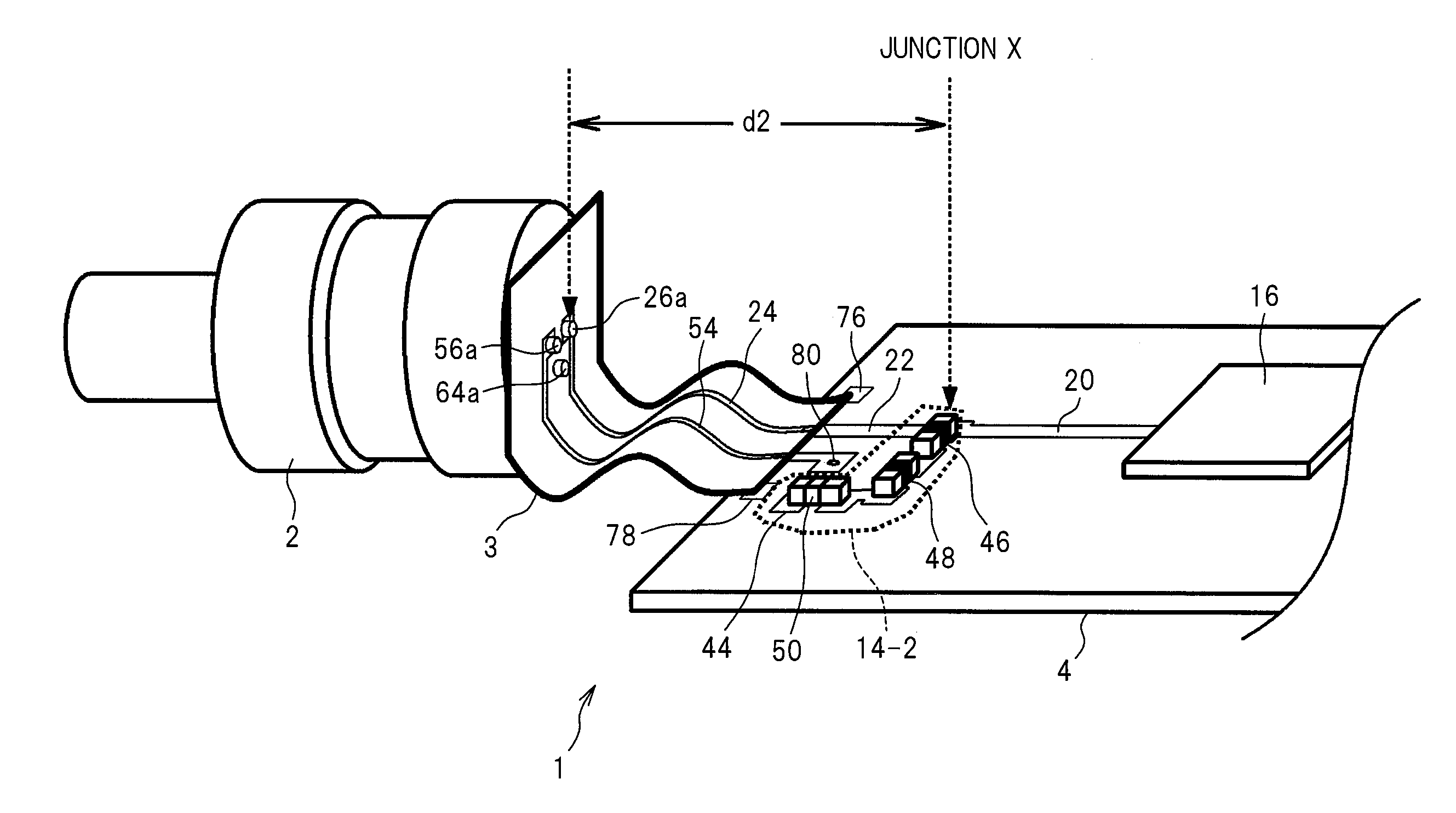
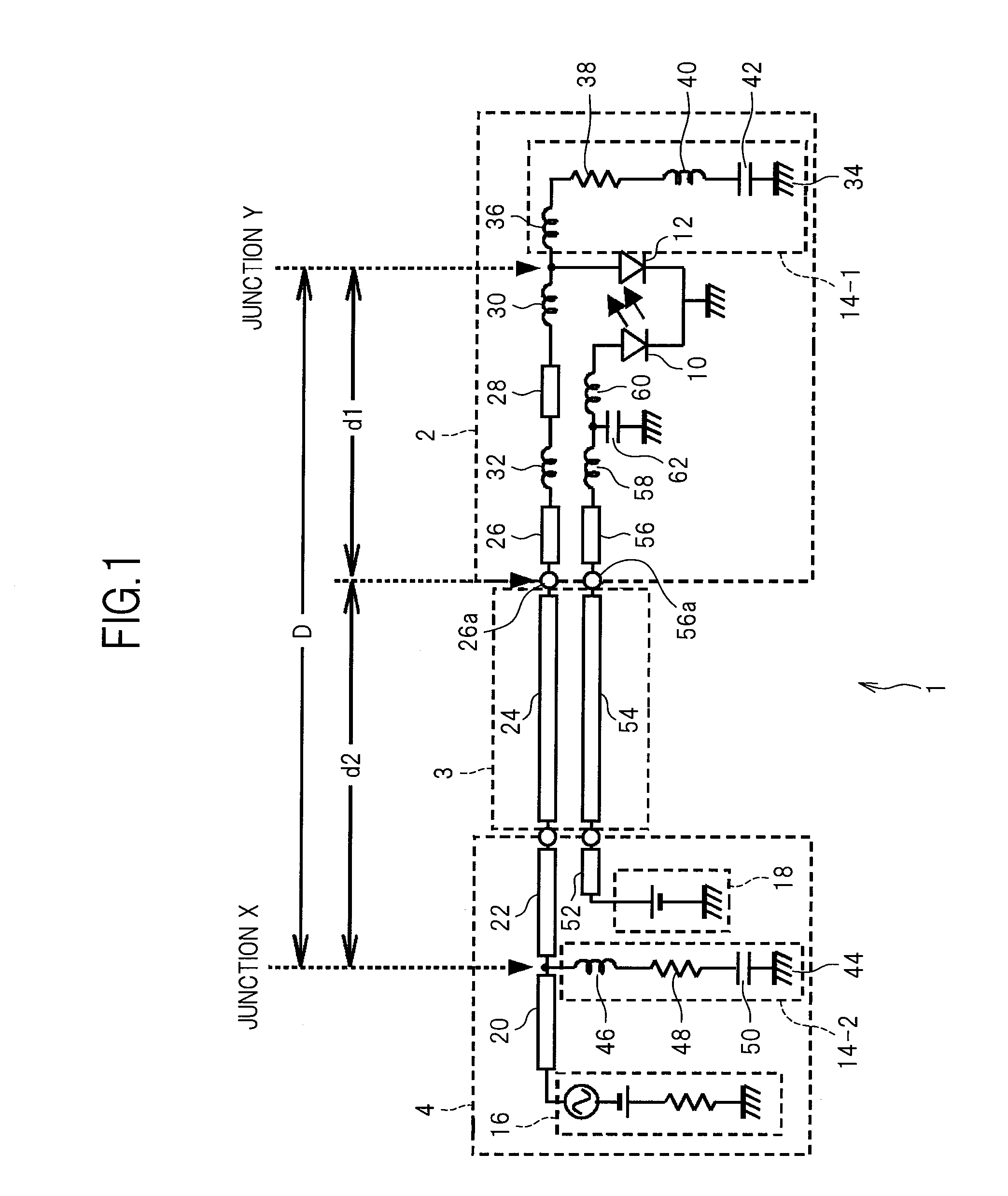
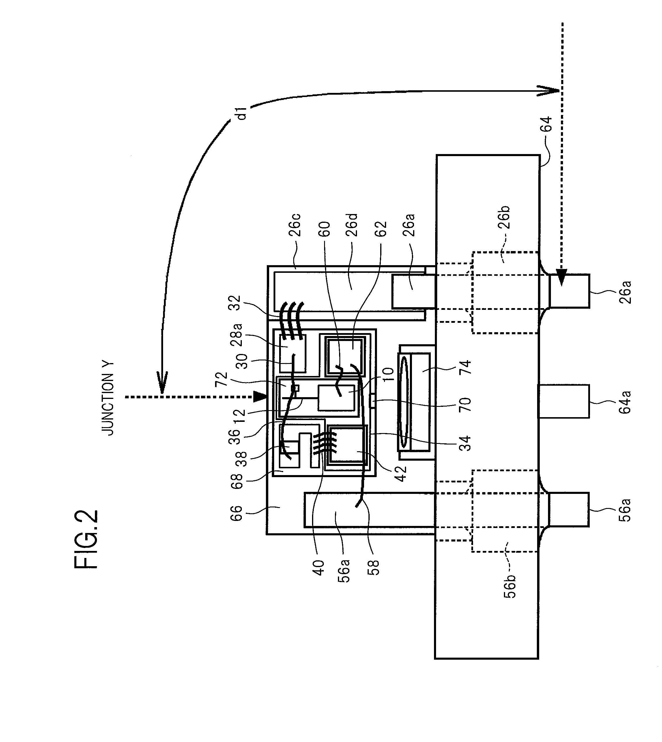
[0035]FIG. 1 is a diagram illustrating an example of major circuits in an optical transmitter device 1 according to this embodiment. FIG. 2 is a diagram illustrating an example of the internal structure of an optical transmitter module 2 which is contained in the optical transmitter device 1 according to this embodiment. FIG. 3 is a diagram illustrating an example of major parts of the optical transmitter device 1 according to this embodiment.

[0036]The optical transmitter device 1 according to this embodiment includes the optical transmitter module 2, a flexible printed board 3, and a printed circuit board 4. The optical transmitter module 2 and the printed circuit board 4 are electrically connected to each other. The optical transmitter module 2 includes a light emitting device (for example, a semiconductor laser diode device 10 in this embodiment), an optical modul...


PUM


Abstract

Provided are an optical transmitter device and an optical transmitter module which are capable of reducing the optical transmitter module size while maintaining a state where an excellent optical transmission waveform quality is obtained over a wide range of frequencies. The optical transmission module (2) includes a semiconductor laser diode device (10), an optical modulator device (12), and a first termination resistor circuit (14-1). A printed circuit board (4) includes a driver IC (16) and a second termination resistor circuit (14-2). A lower cutoff frequency of the first termination resistor circuit (14-1) and an upper cutoff frequency of the second termination resistor circuit (14-2) correspond to each other. An impedance of the first termination resistor circuit (14-1) in a pass frequency band thereof and an impedance of the second termination resistor circuit (14-2) in a pass frequency band thereof correspond to each other.

Description

CROSS-REFERENCE TO RELATED APPLICATION[0001]The present application claims priority from Japanese application JP 2009-062367 filed on Mar. 16, 2009, the content of which is hereby incorporated by reference into this application.BACKGROUND OF THE INVENTION[0002]1. Field of the Invention[0003]The present invention relates to an optical transmitter device and an optical transmitter module.[0004]2. Description of the Related Art[0005]Optical modules with a semiconductor optical modulator device, or an optical modulator-integrated semiconductor laser chip, built in are used as one of the key devices of a transceiver for middle-to-long-distance optical fiber transmission. Optical transceivers have been increased in speed as broadband networks become popular, and now high transmission rate optical transceivers having a bit rate of 10 Gbits / s or higher are widely employed. Optical modules suitable for use in such optical transceivers are demanded to be small in size and low in power consump...

Claims


Application Information

Patent Timeline
Patent Type & Authority Applications(United States)
IPC IPC(8): H04B10/04H01S5/026H04B10/40H04B10/50H04B10/516H04B10/60
CPCH04B10/2504H05K1/0246H05K1/141H05K2201/10121H05K1/189H05K2201/10022H05K1/147H04B10/25891
Inventor KAGAYA, OSAMUMOTOHIRO, SATOSHIHIRAI, MASAHIRO
Owner LUMENTUM JAPAN INC
Why Eureka
Try Eureka