Light-emitting element, light-emitting apparatus, display apparatus, and electronic device

a technology of light-emitting elements and display devices, which is applied in the direction of discharge tubes/lamp details, discharge tubes luminescnet screens, electric discharge lamps, etc., can solve the problems of low contrast, loss of balance, and undesired colors in display devices that include this light-emitting element, and achieve high-contrast images

Active Publication Date: 2010-09-30
SEIKO EPSON CORP
View PDF7 Cites 16 Cited by
  • Summary
  • Abstract
  • Description
  • Claims
  • Application Information

AI Technical Summary

Benefits of technology

[0036]This can provide a reliable electronic device that can display high-contrast images.

Problems solved by technology

However, with a small electric current between the cathode and the anode, balance is lost between the three light-emitting layers of the light-emitting element according to JP-A-2005-100921, and the three light-emitting layers consequently cannot emit white light.
However, white light having an irregular waveform produces red, green, and blue light having an irregular waveform, displaying undesired colors.
Thus, a display apparatus that includes this light-emitting element has a reduced contrast (poor black reproduction).

Method used


Image

  • Light-emitting element, light-emitting apparatus, display apparatus, and electronic device
  • Light-emitting element, light-emitting apparatus, display apparatus, and electronic device
  • Light-emitting element, light-emitting apparatus, display apparatus, and electronic device

Examples


first embodiment

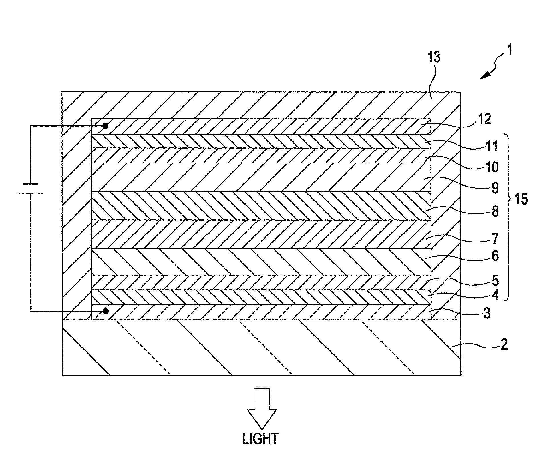
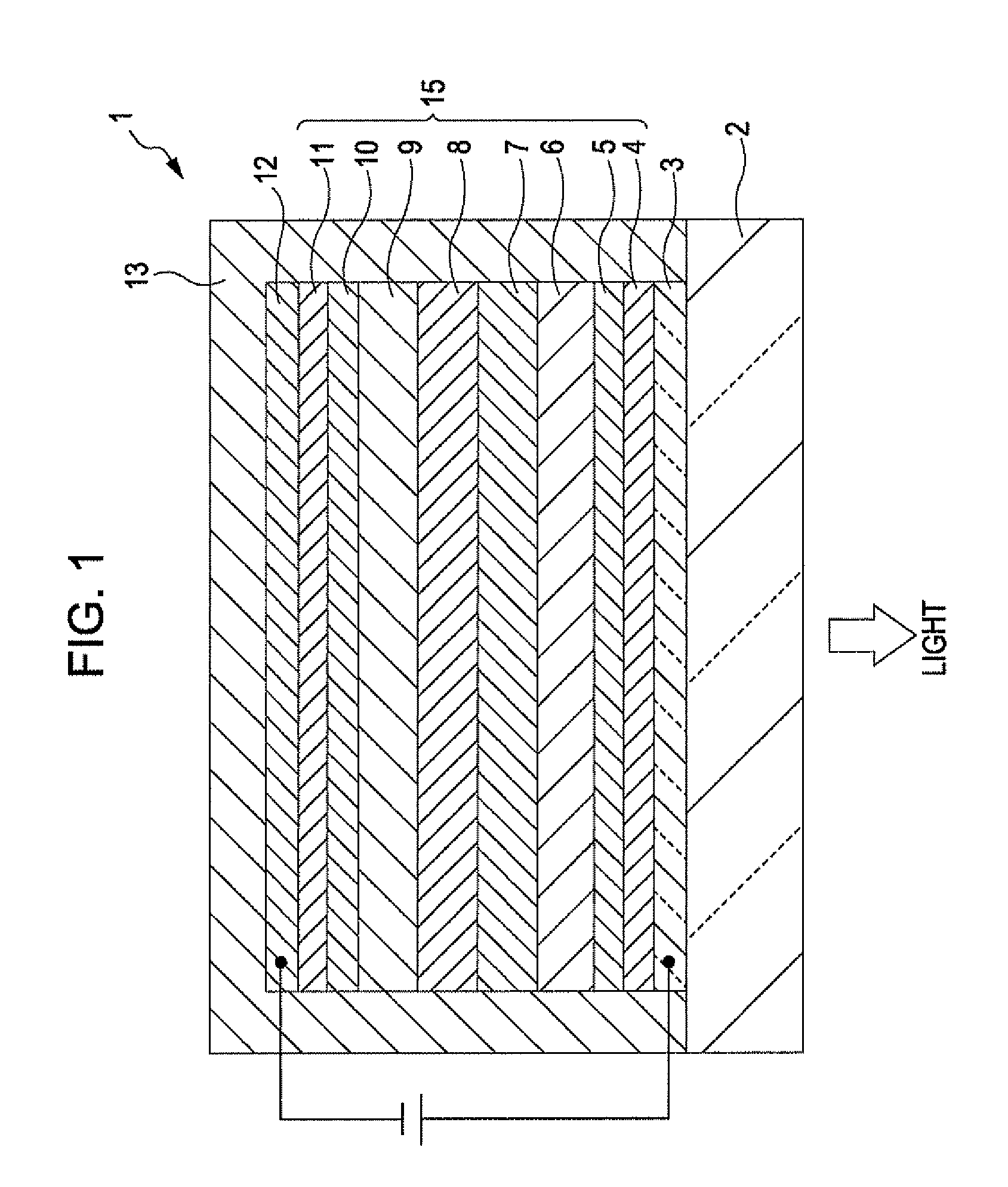
[0046]FIG. 1 is a schematic longitudinal sectional view of a light-emitting element according to a first embodiment of the invention. For convenience of explanation, the top and bottom in FIG. 1 are considered as the “top” and “bottom” of the light-emitting element, respectively.

[0047]A light-emitting element (electroluminescent element) 1 illustrated in FIG. 1 emits white light composed of red (R), green (G), and blue (B) light.

[0048]The light-emitting element 1 includes an anode 3, a hole-injection layer 4, a hole-transport layer 5, a red-light-emitting layer (a first light-emitting layer) 6, an intermediate layer 7, a blue-light-emitting layer (a second light-emitting layer) 8, a green-light-emitting layer (a third light-emitting layer) 9, an electron-transfer layer 10, an electron-injection layer 11, and a cathode 12 layered in this order.

[0049]In other words, the light-emitting element 1 includes a laminate 15 between two electrodes (the anode 3 and the cathode 12). The laminat...

second embodiment

[0180]A second embodiment according to the invention will be described below.

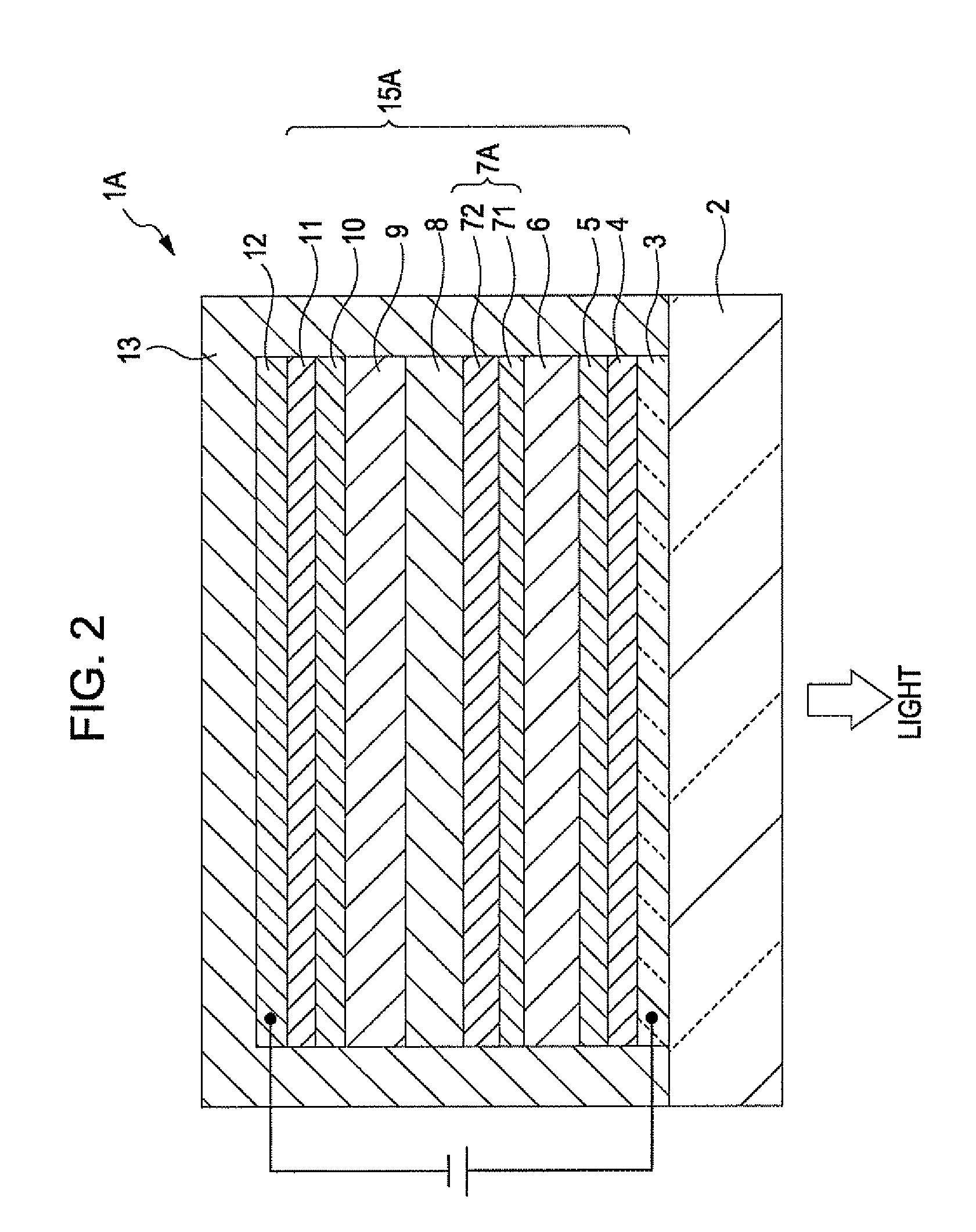
[0181]FIG. 2 is a schematic longitudinal sectional view of a light-emitting element according to a second embodiment of the invention. For convenience of explanation, the top and bottom in FIG. 2 are considered as the “top” and “bottom” of the light-emitting element, respectively.

[0182]A light-emitting element according to the present embodiment is the same as the light-emitting element according to the first embodiment except that the intermediate layer has a different structure.

[0183]The following description relates to the light-emitting element according to the second embodiment and is focused on points of difference from the light-emitting element according to the first embodiment. Thus, their similarities will not be further described.

[0184]A light-emitting element 1A according to the present embodiment includes an intermediate layer 7A between and in contact with the red-light-emitting layer 6 and th...

example 1

[0236](1) First, a transparent glass substrate having an average thickness of 0.5 mm was prepared. An ITO electrode (anode) having an average thickness of 100 nm was formed on the substrate by sputtering.

[0237]The substrate was immersed in acetone and then in 2-propanol and was subjected to ultrasonic cleaning and subsequent oxygen plasma treatment.

(2) A compound having the formula 7 was deposited on the ITO electrode by vacuum evaporation to form a hole-injection layer having an average thickness of 50 nm.

(3) A compound having the formula 16 (a first material) was deposited on the hole-injection layer by vacuum evaporation to form a hole-transport layer having an average thickness of 20 nm.

(4) The material for a red-light-emitting layer was deposited on the hole-transport layer by vacuum evaporation to form a red-light-emitting layer (a first light-emitting layer) having an average thickness of 10 nm. The material for a red-light-emitting layer contained a compound having the formu...


PUM


Abstract

A light-emitting element includes a cathode, an anode, a red-light-emitting layer that is disposed between the cathode and the anode and emits red light, a blue-light-emitting layer that is disposed between the red-light-emitting layer and the cathode and emits blue light, a green-light-emitting layer that is disposed between the blue-light-emitting layer and the cathode and emits green light, and an intermediate layer that is disposed between and in contact with the red-light-emitting layer and the blue-light-emitting layer and functions so as to control the transfer of positive holes and electrons between the red-light-emitting layer and the blue-light-emitting layer, wherein the intermediate layer contains a first material and a second material different from the first material, the red-light-emitting layer contains a material of the same type as the first material, and each of the blue-light-emitting layer and the green-light-emitting layer contains a material of the same type as the second material.

Description

BACKGROUND[0001]1. Technical Field[0002]The present invention relates to a light-emitting element, a light-emitting apparatus, a display apparatus, and an electronic device.[0003]2. Related Art[0004]Organic electroluminescent elements (organic EL elements) are light-emitting elements that include at least one organic light-emitting layer between an anode and a cathode. Upon the application of an electric field between the cathode and the anode, electrons in the cathode and positive holes in the anode are transferred to the light-emitting layer and recombine with each other in the light-emitting layer, generating excitons. When excitons return to the ground state, excitons release the excitation energy as light.[0005]One example of such light-emitting elements includes three light-emitting layers corresponding to red (R), green (G), and blue (B) between a cathode and an anode and emits white light (see, for example, JP-A-2005-100921). Such a white-light-emitting element can be used i...

Claims


Application Information

Patent Timeline
Patent Type & Authority Applications(United States)
IPC IPC(8): H01J1/62
CPCH01L27/3246H01L51/0054H01L51/0057H01L51/5044H01L51/0059H01L51/0071H01L51/504H01L51/0058H10K59/122H10K85/622H10K85/625H10K85/631H10K85/626H10K85/657H10K50/131H10K50/13
Inventor FUJITA, TETSUJIYAMAMOTO, HIDETOSHIMITSUHASHI, ETSUO
Owner SEIKO EPSON CORP
Why Eureka
Try Eureka