Tandem white OLED with efficient electron transfer

a light-producing oled, tandem technology, applied in the direction of discharge tube luminescnet screen, organic chemistry, natural mineral layered products, etc., can solve the problems of difficult to achieve light emission with strong intensity, tandem white oled device has weak green and red color components in the spectrum, and achieves low voltage requirement , good color emission

Active Publication Date: 2010-10-07
GLOBAL OLED TECH
View PDF24 Cites 25 Cited by
  • Summary
  • Abstract
  • Description
  • Claims
  • Application Information

AI Technical Summary

Benefits of technology

[0014]It is an advantage of this invention that it can provide a display with increased efficiency while maintaining good color emission and a low voltage requirement.

Problems solved by technology

This produces manufacturing difficulties.
However, it is difficult to achieve light emission with strong intensity in the red, green, and blue portions of the spectrum.
Although luminance efficiency is increased, this tandem white OLED device has weaker green and red color components in the spectrum.

Method used


Image

  • Tandem white OLED with efficient electron transfer
  • Tandem white OLED with efficient electron transfer
  • Tandem white OLED with efficient electron transfer

Examples


example 1

Comparative

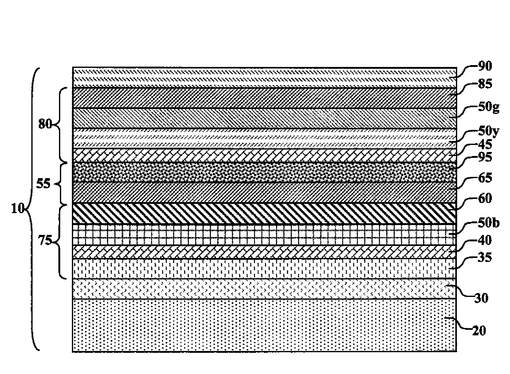
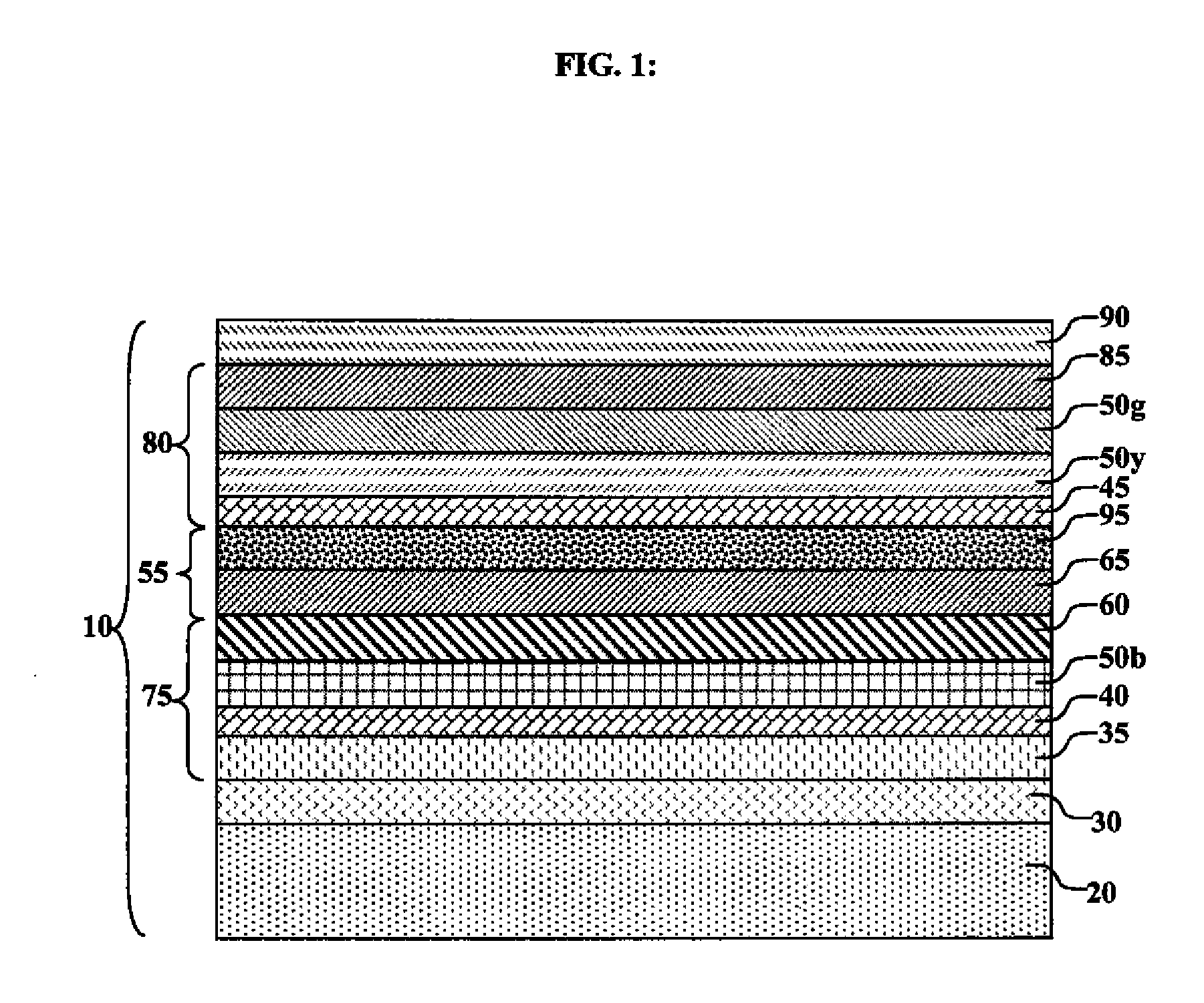
[0113]1. A clean glass substrate was deposited by sputtering with indium tin oxide (ITO) to form a transparent electrode of 60 nm thickness.[0114]2. The above-prepared ITO surface was treated with a plasma oxygen etch.[0115]3. The above-prepared substrate was further treated by vacuum-depositing a 10 nm layer of hexacyanohexaazatriphenylene (CHATP) as a hole-injecting layer (HIL).

[0116]4. The above-prepared substrate was further treated by vacuum-depositing a 150 nm layer of 4,4′-bis[N-(1-naphthyl)-N-phenylamino]biphenyl (NPB) as a hole-transporting layer (HTL).[0117]5. The above-prepared substrate was further treated by vacuum-depositing a 30 nm blue light-emitting layer including 95% 9-(1-naphthyl)-10-(2-naphthyl)anthracene (NNA) host with 5% BED-1 as blue-ernitting dopant.

[0118]6. A 40 nm mixed lithium-doped n-type layer was vacuum-deposited, including 49% 4,7-diphenyl-1,10-phenanthroline (also known as bathophen or Bphen), 49% lithium quinolinolate (LiQ) as co-host, w...

example 2

Comparative

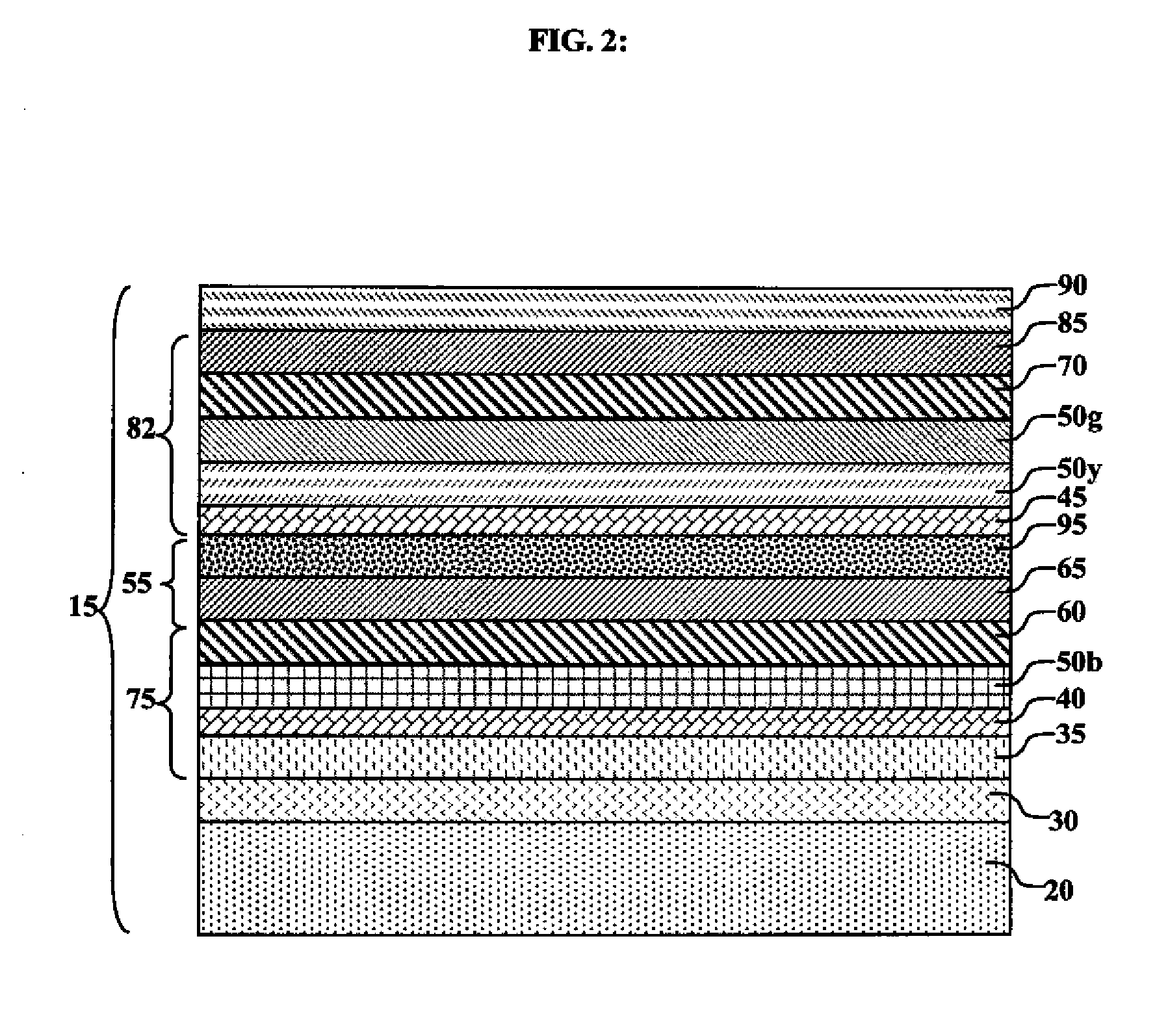
[0125]An OLED device was constructed as described above for Example 1 except that Step 10a was added after Step 10 and Step 11 was modified as follows to keep the same overall device thickness:[0126]10a. The above-prepared substrate was further treated by vacuum-depositing a 10 nm layer of 3,7,10-triphenyl-8-(4-biphenyl)fluoranthene (ETM-2, as described above) to form a fluoranthene-containing electron-transporting layer.[0127]11. A 24 nm mixed lithium-doped electron-transporting layer was vacuum-deposited, including 49% Bphen and 49% LiQ as co-hosts, with 2% Li metal.

example 3

Inventive

[0128]An OLED device was constructed as described above for Example 1 except that Step 5a was added after Step 5 and Step 6 was modified as follows to keep the same overall device thickness:[0129]5a. The above-prepared substrate was further treated by vacuum-depositing a 10 nm layer of ETM-2 to form a fluoranthene-containing electron-transporting layer.[0130]6. A 30 nm mixed lithium-doped n-type layer was vacuum-deposited, including 49% Bphen, 49% LiQ as co-host, with 2% Li metal.


PUM

PropertyMeasurementUnit
wavelengthsaaaaaaaaaa

Abstract

A white-light-emitting tandem OLED device having spaced anode and cathode including: first and second light-emitting units disposed between the anode and cathode; an intermediate connector including an n-type layer and a p-type layer disposed between the first and second light-emitting units; and a fluoranthene-containing electron-transporting layer adjacent to the n-type layer of the intermediate connector and including at least 25% of a 7,10-diaryl-substituted fluoranthene compound having no aromatic rings annulated to the fluoranthene nucleus.

Description

CROSS REFERENCE TO RELATED APPLICATION[0001]Reference is made to commonly assigned U.S. patent application Ser. No. 11 / 924,631 filed Oct. 26, 2007, entitled “OLED Device With Electron Transport Materials” by Begley, the disclosure of which is incorporated herein by reference.FIELD OF THE INVENTION[0002]The present invention relates to broadband light-producing OLED displays suitable for large displays.BACKGROUND OF THE INVENTION[0003]An organic light-emitting diode device, also called an OLED, commonly includes an anode, a cathode, and an organic electroluminescent (EL) unit sandwiched between the anode and the cathode. The organic EL unit includes at least a hole-transporting layer (HTL), a light-emitting layer (LEL), and an electron-transporting layer (ETL). OLEDs are attractive because of their low drive voltage, high luminance, wide viewing-angle, and capability for full color displays and for other applications. Tang et al. described this multilayer OLED in their U.S. Pat. Nos....

Claims


Application Information

Patent Timeline
Patent Type & Authority Applications(United States)
IPC IPC(8): H01J1/63
CPCH01L51/0054H01L51/0059H01L51/5278H01L51/0077H01L51/5048H01L51/0072H10K85/622H10K85/631H10K85/30H10K85/6572H10K50/14H10K50/19C07C13/62H10K50/00
Inventor SPINDLER, JEFFREY P.HATWAR, TUKARAM K.BEGLEY, WILLIAM J.
Owner GLOBAL OLED TECH
Why Eureka
Try Eureka