Pixel Driver Circuits

a driver circuit and pixel technology, applied in the direction of electrical equipment, instruments, electric digital data processing, etc., can solve the problems of difficult to predict the brightness of a pixel, and achieve the effect of facilitating the fabrication of pixel circuits, increasing operating efficiency, and ensuring the operation of circuits

Inactive Publication Date: 2010-10-07
CAMBRIDGE DISPLAY TECH LTD
View PDF10 Cites 45 Cited by
  • Summary
  • Abstract
  • Description
  • Claims
  • Application Information

AI Technical Summary

Benefits of technology

[0013]In embodiments with two capacitively coupled input terminals the additional flexibility afforded by the second input terminal facilitates the fabrication of pixel circuits with an increased operating efficiency and / or the ability for greater control of the operation of the circuit. Thus in embodiments one of the input terminals and its associated capacitance may be employed for compensation of pixel brightness and / or colour for one or more of aging, temperature and positional non-uniformity. An input terminal may be employed to tune one or more parameters of the pixel circuit and / or to programme the pixel circuit to set a pixel brightness (here brightness includes the brightness of a colour sub-pixel of a multicolour display).
[0014]In still further embodiments the additional capacitively coupled input terminal may be employed to provide compensation for mis-match between devices, for example to compensate for variations due to device mis-match in a current mirror based pixel circuit.
[0015]In still other pixel circuits the effective threshold voltage of a FG thin film transistor may be reduced to zero or even inverted by applying a voltage to one (or more) of the capacitively coupled input terminals of the FG transistor. This can reduce the input voltage required for a given drain-source current, thus reducing the required drain-source voltage (Vds), in particular if it is preferred that the device operates in saturation. This can therefore reduce power requirements and increase operating efficiency.
[0016]Furthermore, ability to change the effective threshold voltage is beneficial for circuits that need tuning and programming, where mismatch needs to be corrected between adjacent transistors.

Problems solved by technology

It is common to provide a current-programmed drive to an OLED because the brightness of an OLED is determined by the current flowing through the device, this determining the number of photons it generates, whereas in a simple voltage-programmed configuration it can be difficult to predict how bright a pixel will appear when driven.

Method used


Image

  • Pixel Driver Circuits
  • Pixel Driver Circuits
  • Pixel Driver Circuits

Examples


Embodiment Construction

Active Matrix Pixel Circuits

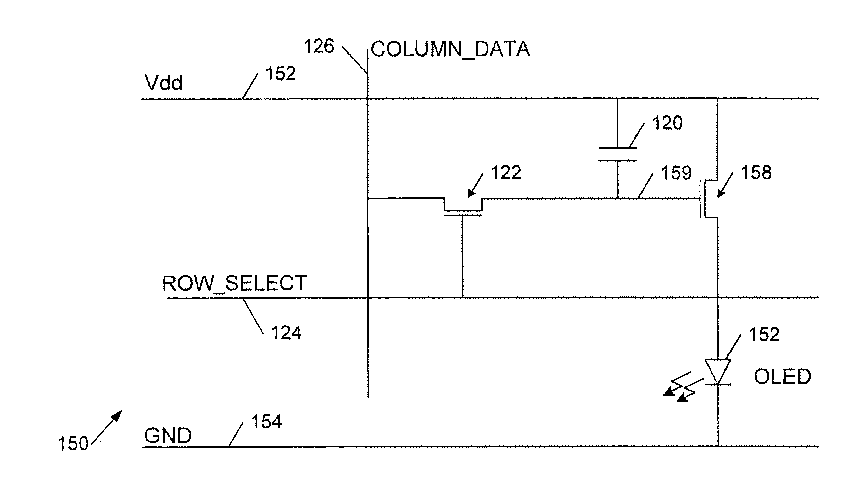
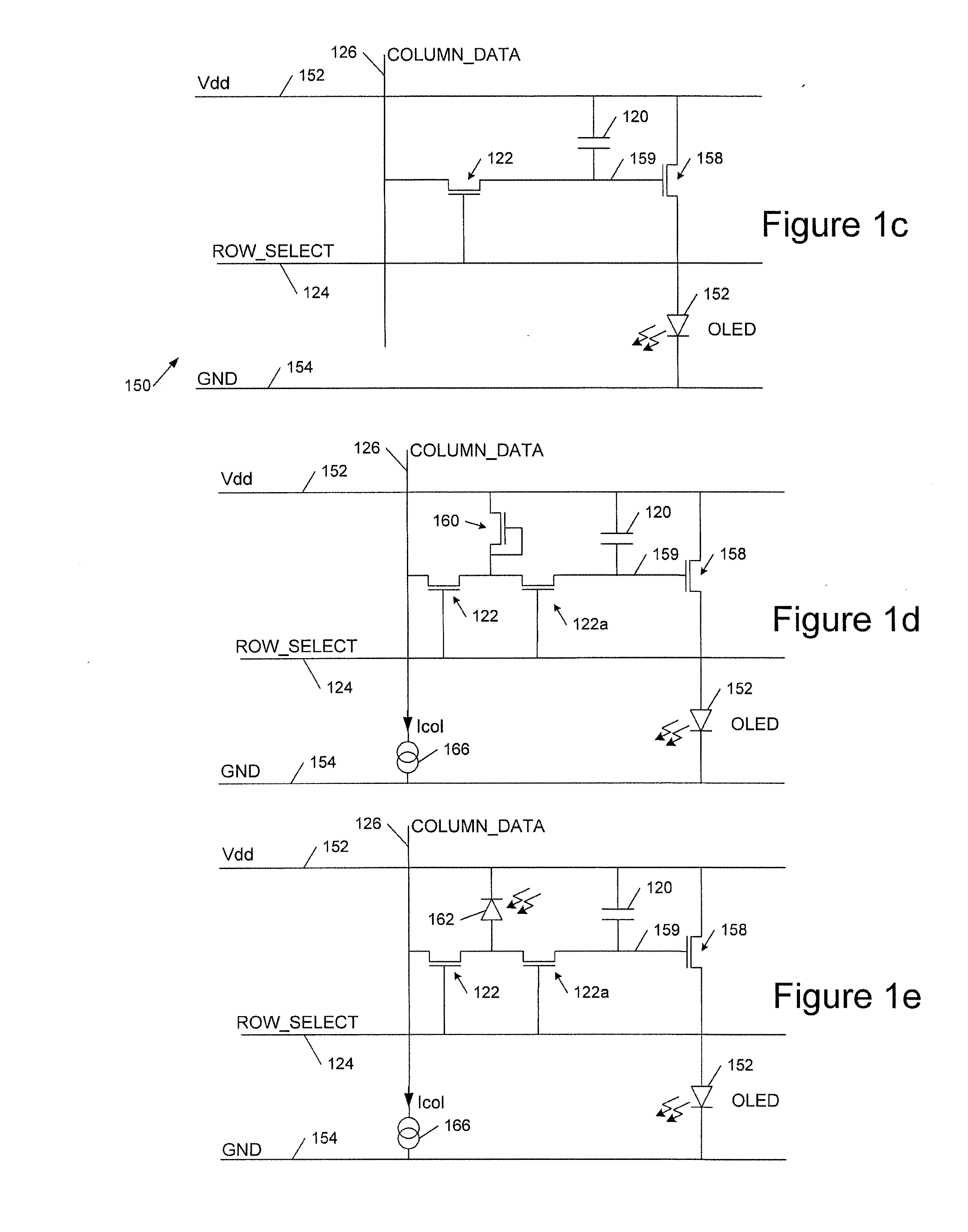
[0037]FIG. 1c shows an example of a voltage programmed OLED active matrix pixel circuit 150. A circuit 150 is provided for each pixel of the display and Vdd 152, Ground 154, row select 124 and column data 126 busbars are provided interconnecting the pixels. Thus each pixel has a power and ground connection and each row of pixels has a common row select line 124 and each column of pixels has a common data line 126.

[0038]Each pixel has an OLED 152 connected in series with a driver transistor 158 between ground and power lines 152 and 154. A gate connection 159 of driver transistor 158 is coupled to a storage capacitor 120 and a control transistor 122 couples gate 159 to column data line 126 under control of row select line 124. Transistor 122 is a thin film field effect transistor (TFT) switch which connects column data line 126 to gate 159 and capacitor 120 when row select line 124 is activated. Thus when switch 122 is on a voltage on column data line 126 ...


PUM


Abstract

This invention relates to pixel driver circuits for active matrix optoelectronic devices, in particular OLED (organic light emitting diodes) displays. We describe an active matrix optoelectronic device having a plurality of active matrix pixels each said pixel including a pixel circuit comprising a thin film transistor (TFT) for driving the pixel and a pixel capacitor for storing a pixel value, wherein said TFT comprises a TFT with a floating gate.

Description

FIELD OF THE INVENTION[0001]This invention relates to pixel driver circuits for active matrix optoelectronic devices, in particular OLED (organic light emitting diodes) displays.BACKGROUND TO THE INVENTION[0002]Embodiments of the invention will be described while particularly useful in active matrix OLED displays although applications and embodiments of the invention are not limited to such displays and may be employed with other types of active matrix display and also, in embodiments, in active matrix sensor arrays.Organic Light Emitting Diode Displays[0003]Organic light emitting diodes, which here include organometallic LEDs, may be fabricated using materials including polymers, small molecules and dendrimers, in a range of colours which depend upon the materials employed. Examples of polymer-based organic LEDs are described in WO 90 / 13148, WO 95 / 06400 and WO 99 / 48160; examples of dendrimer-based materials are described in WO 99 / 21935 and WO 02 / 067343; and examples of so called sm...

Claims


Application Information

Patent Timeline
Patent Type & Authority Applications(United States)
IPC IPC(8): G09G3/30G09G5/00G09G5/10H01L51/10H05B44/00
CPCG09G3/3233G09G3/325G09G3/3283G09G3/3291G09G2300/0465G09G2360/148G09G2300/0852G09G2300/0861G09G2300/0876G09G2310/0256G09G2320/043G09G2300/0819G09G3/32G09G3/3225
Inventor RANKOV, ALEKSANDRASMITH, EUAN CHRISTOPHER
Owner CAMBRIDGE DISPLAY TECH LTD
Why Eureka
Try Eureka