Semiconductor Device and Method for Manufacturing the Same
a semiconductor device and semiconductor technology, applied in the direction of semiconductor devices, electrical devices, transistors, etc., can solve the problems of difficult to form n-channel transistors and p-channel transistors using the same material, and achieve the effect of reducing the cost of manufacturing a semiconductor device, improving the characteristics of a semiconductor device, and suppressing the use of a large number of masks
- Summary
- Abstract
- Description
- Claims
- Application Information
AI Technical Summary
Benefits of technology
Problems solved by technology
Method used
Image

Examples
embodiment 1
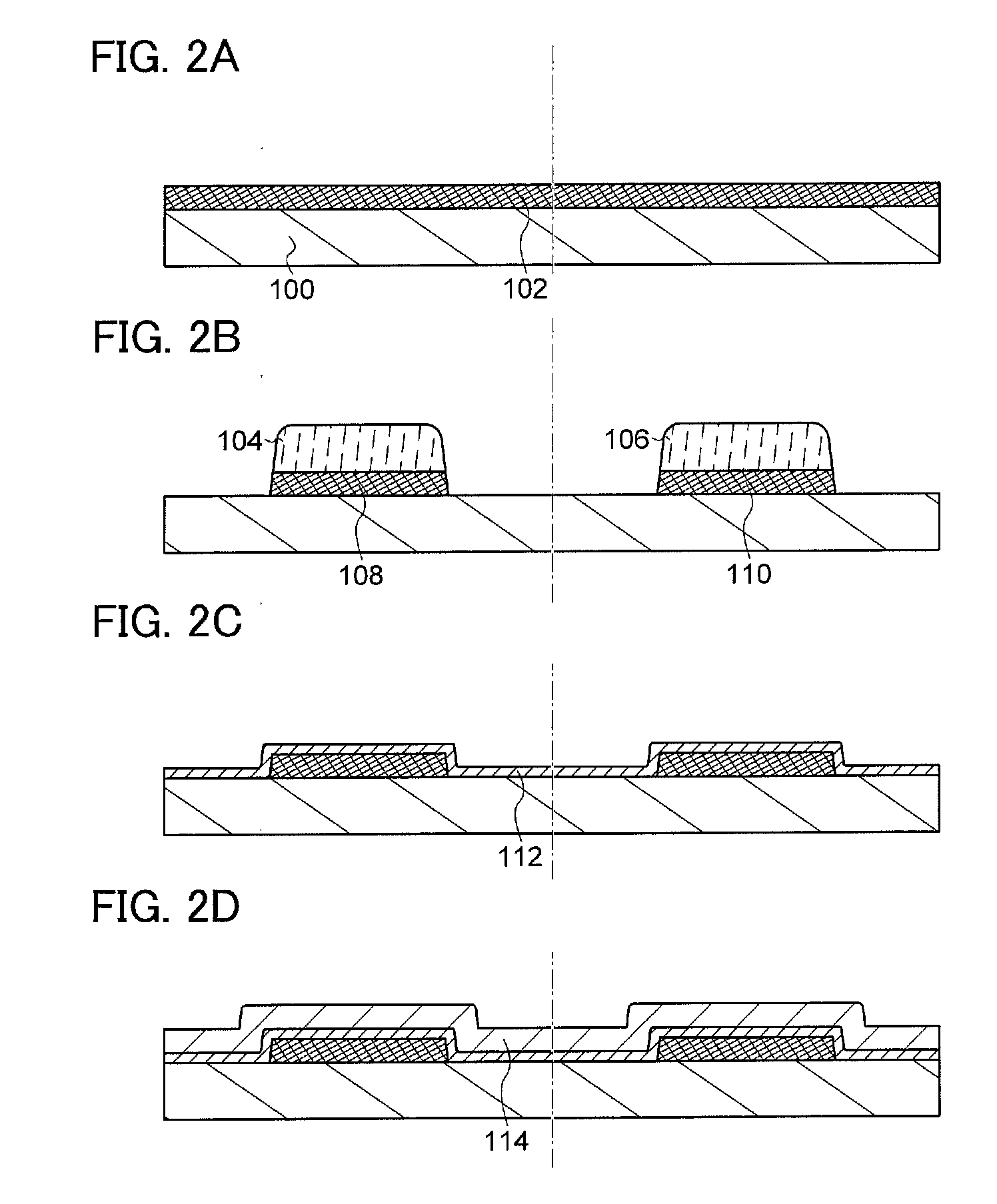
[0051]In this embodiment, an example of a structure of a semiconductor device is described with reference to FIGS. 1A and 1B, and an example of a method for manufacturing a semiconductor device is described with reference to FIGS. 2A to 2D, FIGS. 3A to 3D, and FIGS. 4A to 4D.
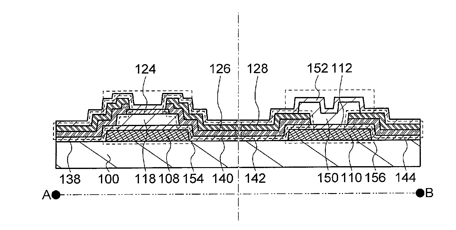
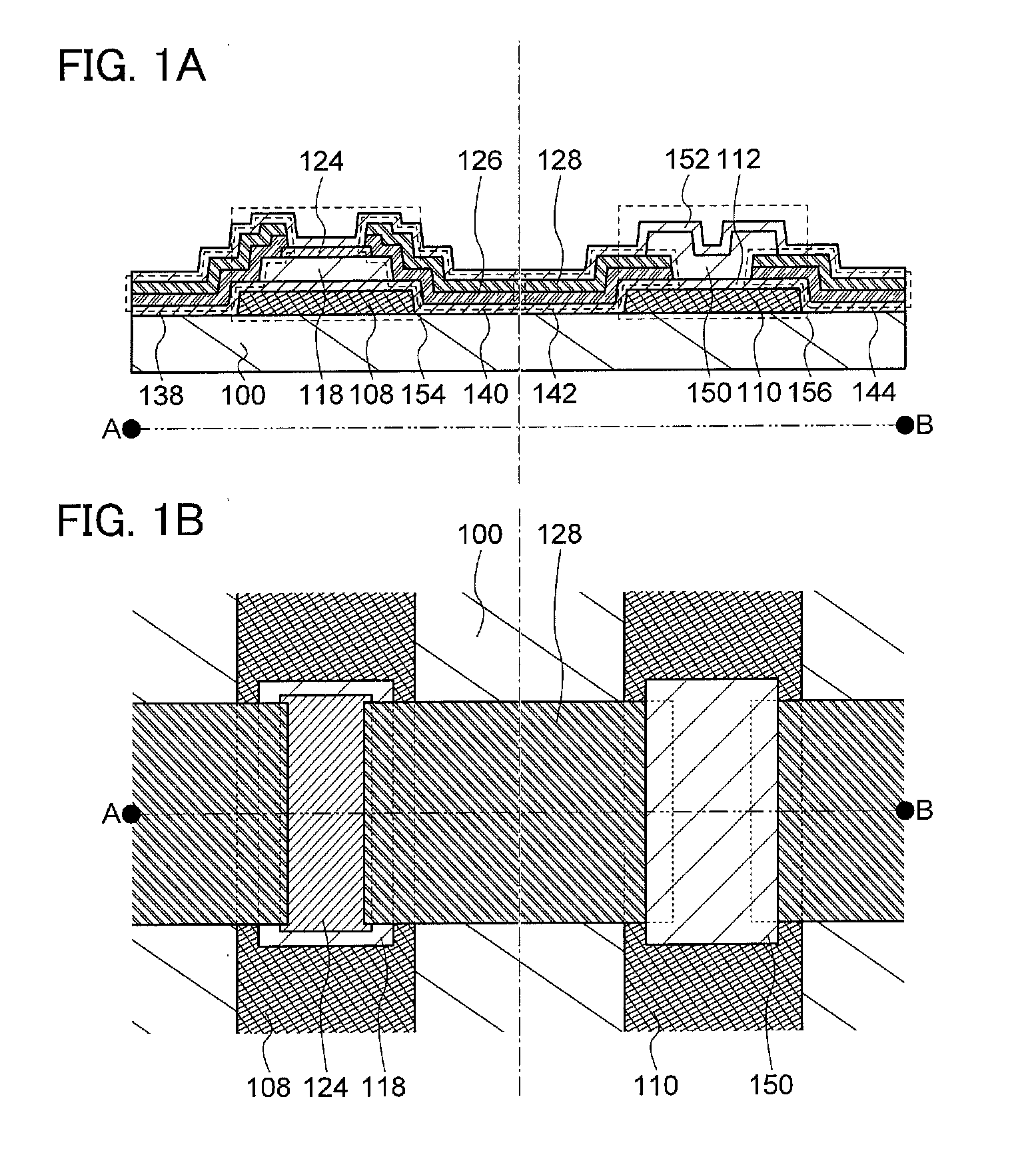
[0052]FIGS. 1A and 1B illustrate the example of the structure of the semiconductor device according to Embodiment 1. FIG lA is a cross-sectional view, and FIG. 1B is a plan view. FIG. 1A illustrates a cross section taken along line A-B in FIG. 1B. Note that in the plan view, part of the structure is omitted for simplicity.
[0053]The semiconductor device illustrated in FIGS. 1A and 1B relates to a first transistor 154 and a second transistor 156 each using an oxide semiconductor and includes a substrate 100 (for example, a substrate having an insulating surface); a first gate electrode 108 and a second gate electrode 110 over the substrate 100; a gate insulating layer 112 covering the first gate electrode 108 and ...
embodiment 2
[0097]In Embodiment 2, another example of a structure of a semiconductor device is described with reference to FIGS. 5A and 5B, and another example of a method for manufacturing a semiconductor device is described with reference to FIGS. 6A to 6E. Note that the structure of a semiconductor device to be described in Embodiment 2 has a lot in common with the structure of the semiconductor device described in Embodiment 1. Therefore, portions different from those in Embodiment 1 are mainly described below.
[0098]FIGS. 5A and 5B illustrate an example of a structure of a semiconductor device according to Embodiment 2. FIG. 5A is a cross-sectional view, and FIG. 5B is a plan view. FIG. 5A illustrates a cross section taken along line A-B in FIG. 5B. Note that in the plan view, part of the structure is omitted for simplicity.
[0099]A semiconductor device illustrated in FIGS. 5A and 5B relates to a first transistor 228 and a second transistor 230 using an oxide semiconductor and includes the s...
embodiment 3
[0112]In Embodiment 3, another example of a structure of a semiconductor device is described with reference to FIGS. 7A and 7B, and another example of a method for manufacturing a semiconductor device is described with reference to FIGS. 8A to 8D and FIGS. 9A to 9C. Note that the structure of a semiconductor device to be described in Embodiment 3 has a lot in common with the structures of the semiconductor devices described in Embodiments 1 and 2. Therefore, portions different from Embodiments 1 and 2 are mainly described below.
[0113]FIGS. 7A and 7B illustrate an example of a structure of a semiconductor device according to Embodiment 3. FIG. 7A is a cross-sectional view, and FIG. 7B is a plan view. Note that FIG. 7A illustrates a cross section taken along line A-B in FIG. 7B. Note that in the plan view, part of the structure is omitted for simplicity.
[0114]The semiconductor device illustrated in FIGS. 7A and 7B relates to a first transistor 322 and a second transistor 324 each usin...
PUM
 Abstract
Description
Claims
Application Information
 - R&D
- Intellectual Property
- Life Sciences
- Materials
- Tech Scout
- Unparalleled Data Quality
- Higher Quality Content
- 60% Fewer Hallucinations
Browse by: Latest US Patents, China's latest patents, Technical Efficacy Thesaurus, Application Domain, Technology Topic, Popular Technical Reports.
© 2025 PatSnap. All rights reserved.Legal|Privacy policy|Modern Slavery Act Transparency Statement|Sitemap|About US| Contact US: help@patsnap.com