Electronic ballast with input voltage fault control

a technology of fault control and electronic ballast, which is applied in the field of electronic ballasts, can solve the problems of switch off, and insufficient energy storage in the inductor

Inactive Publication Date: 2010-10-28
PANASONIC INTELLECTUAL PROPERTY MANAGEMENT CO LTD
View PDF5 Cites 14 Cited by
  • Summary
  • Abstract
  • Description
  • Claims
  • Application Information

AI Technical Summary

Benefits of technology

[0012]The present invention is made in consideration of the above-described issue and has as one objective to provide a ballast that can prevent a switch from being damaged when an abnormality occurs in the output voltage of the input power supply.

Problems solved by technology

In a conventional step-up or boost chopper circuit, if the output voltage of the input power supply is temporarily reduced, sufficient energy is not stored in the inductor even if the switch is turned on.
However, as described above, the predetermined value of the current through the switch is set lower, and therefore by erroneously detecting the current during the reverse recovery time of the diode as the switching current through the switch, the switch is turned off with energy storage in the inductor being insufficient.
As a result, because energy stored in the inductor is insufficient, the stored energy is immediately released, and the zero current detection circuit having detected the release, turns on the switch.
For this reason, if the abnormality of the input power supply continues, the switch may repeat on / off switching in a very short period, specifically, on a nanosecond basis, which may thermally damage the switch due to an increase in switching losses.

Method used


Image

  • Electronic ballast with input voltage fault control
  • Electronic ballast with input voltage fault control
  • Electronic ballast with input voltage fault control

Examples


first embodiment

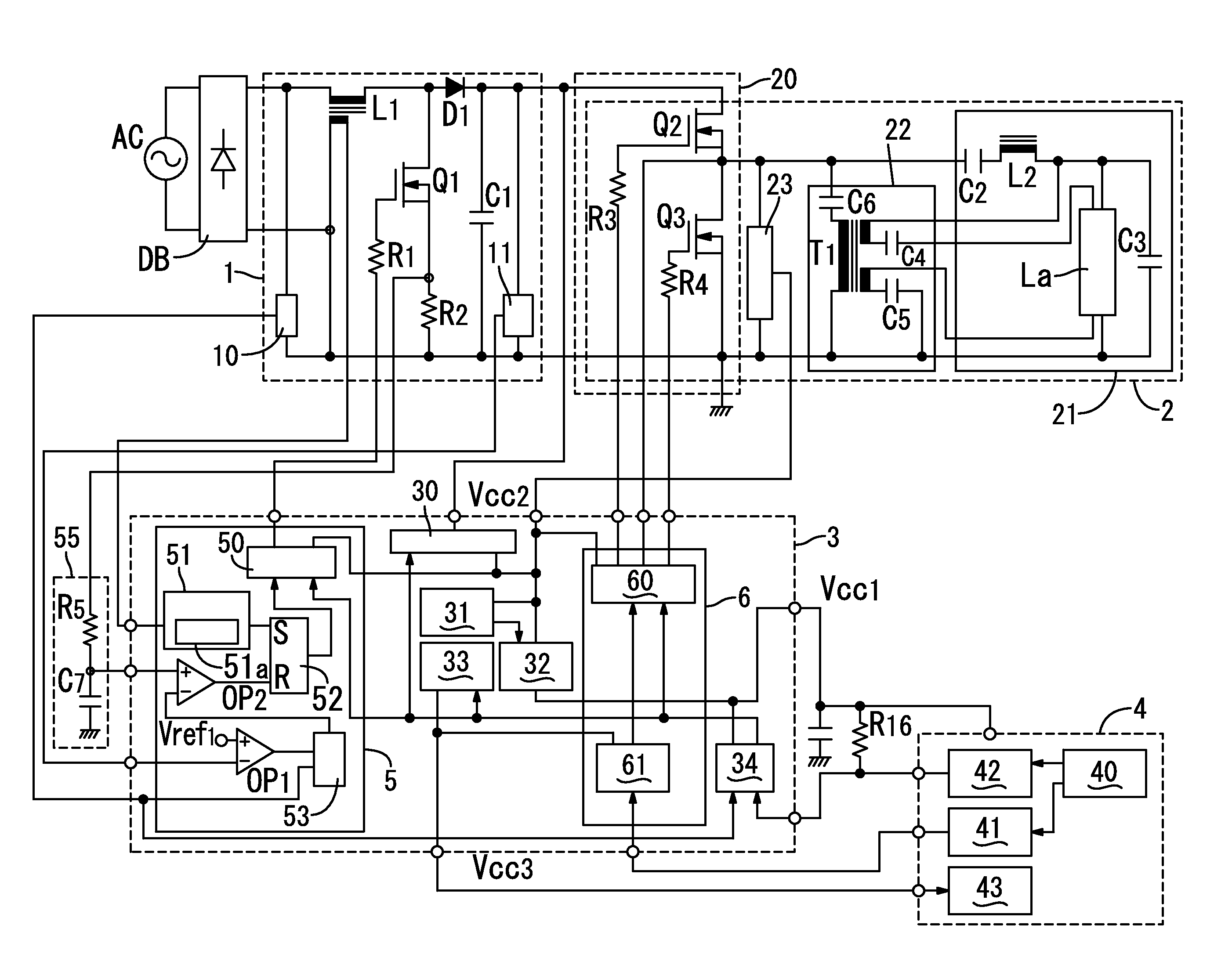
[0042]a electronic ballast according to the present invention is described below with reference to FIG. 1 of the drawings. In the present embodiment, as will be described later, a load circuit 2 includes an inverter circuit 20 that converts a DC voltage from a DC power supply circuit 1 to a high frequency voltage. A resonant circuit 21 receives the high frequency voltage from the inverter circuit 20 to light the discharge lamp La by resonance action. The load circuit 2 is configured to supply lighting power to the discharge lamp La. However, the load circuit 2 is not limited to the illustrated embodiment but may be configured to supply operating power to a load (for example, in the case of an illumination light source, a light emitting diode, or the like) other than a discharge lamp La.

[0043]The present embodiment further includes, as shown in FIG. 1, a rectifier circuit DB including a diode bridge that rectifies an AC voltage from an AC power supply AC to output a ripple voltage an...

fourth embodiment

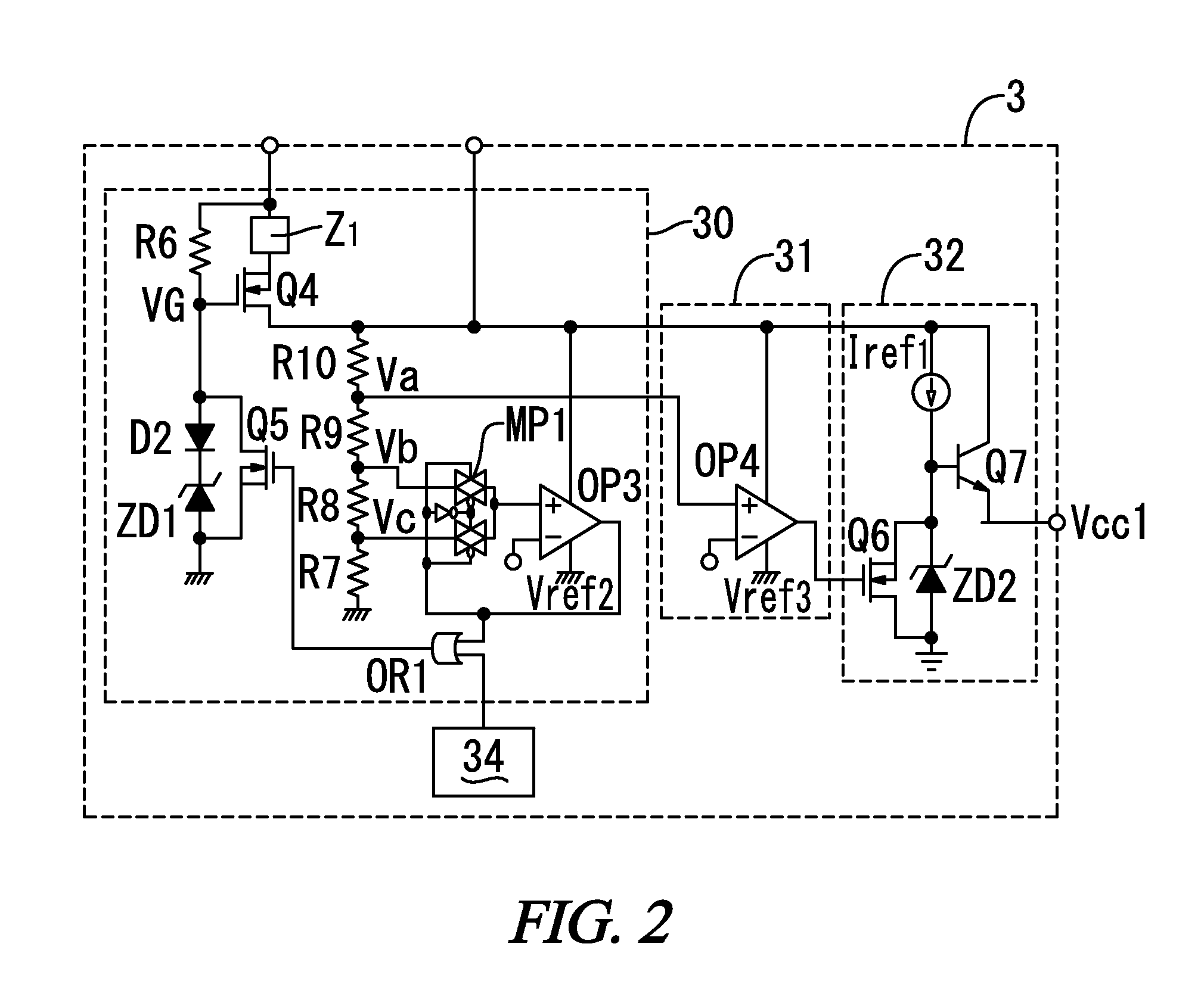
[0113]the electronic ballast according to the present invention is described below with reference to FIG. 18. Note that the basic configuration of the present embodiment is in common with the first or second embodiment, and therefore common circuits are denoted by the same reference numerals to omit description. The present embodiment includes a voltage rise detection circuit 57 that is provided in the DC power supply control circuit 5 and determines whether or not the output voltage of the DC power supply circuit 1 exceeds a first predetermined over-voltage higher than the target voltage. This embodiment further includes a lamp end of life detection circuit 7 and a first abnormality detection circuit 44. The end of life detection circuit 7 and the first abnormality detection circuit 44 have the same configurations as those of the third embodiment 3.

[0114]The voltage rise detection circuit 57 includes, as illustrated in FIG. 19, a third multiplexer circuit MP3 having a pair of trans...


PUM


Abstract

An electronic ballast includes circuitry to prevent a switch from being damaged in the case where an abnormality occurs in an output voltage of an input power supply. A DC power supply control circuit has a zero current detection circuit that, when a current through an inductor becomes equal to or less than a predetermined current value, outputs a zero signal. A peak current detection circuit, when current through a switch the DC power supply circuit becomes equal to or greater than the predetermined current value, outputs a peak signal. A first drive circuit turns on the switch according to the zero signal, and turns off the switch Q1 according to the peak signal. The zero current detection circuit is provided with a mask circuit that stops the zero signal from being outputted to the first drive circuit for a predetermined period after the current through the inductor has become equal to or less than the predetermined current value.

Description

[0001]A portion of the disclosure of this patent document contains material that is subject to copyright protection. The copyright owner has no objection to the reproduction of the patent document or the patent disclosure, as it appears in the U.S. Patent and Trademark Office patent file or records, but otherwise reserves all copyright rights whatsoever.CROSS-REFERENCES TO RELATED APPLICATIONS[0002]This application claims benefit of the following patent application(s) which is / are hereby incorporated by reference: Japan Patent Application No. 2009-107071, filed Apr. 24, 2009.STATEMENT REGARDING FEDERALLY SPONSORED RESEARCH OR DEVELOPMENT[0003]Not ApplicableREFERENCE TO SEQUENCE LISTING OR COMPUTER PROGRAM LISTING APPENDIX[0004]Not ApplicableBACKGROUND OF THE INVENTION[0005]The present invention relates to electronic ballasts that supply operating power to a load such as a gas discharge lamp.[0006]Conventional electronic ballasts convert a DC voltage from a DC power supply or an AC v...

Claims


Application Information

Patent Timeline
Patent Type & Authority Applications(United States)
IPC IPC(8): H05B37/02
CPCH05B41/2856H05B33/0887H05B45/50
Inventor ONISHI, NAOKIASANO, HIROYUKIHAMANA, TETSUYAYAMANAKA, MASAHIRO
Owner PANASONIC INTELLECTUAL PROPERTY MANAGEMENT CO LTD
Why Eureka
Try Eureka