Bifacial solar cells with back surface doping

a solar cell and back surface technology, applied in the field of solar cells, can solve the problems of relatively complex design and technology, and thus high cost, and achieve the effect of reducing manufacturing costs, and simplifying the manufacturing process

Inactive Publication Date: 2010-11-04
HIGHLAND MATERIALS INC
View PDF15 Cites 25 Cited by
  • Summary
  • Abstract
  • Description
  • Claims
  • Application Information

AI Technical Summary

Benefits of technology

[0007]The present invention provides a simplified manufacturing process and the resultant bifacial solar cell (BSC), the simplified manufacturing process reducing manufacturing costs. In at least one embodiment of the invention, a manufacturing method is provided that is comprised of the steps of depositing a boron doped layer onto the back surface of a p-type silicon substrate, depositing a back surface dielectric over the boron doped layer, diffusing phosphorous onto the front surface of the silicon substrate to form an n+ layer and a front surface junction, removing the phosphor-silicate glass formed during the diffusion step (e.g., by etching with HF), depositing a front surface passivation and AR dielectric layer onto the n+ layer, applying front and back surface contact grids, firing the front and back surface contact grids, and isolating the front surface junction, for example using a laser scriber. The front and back surface contact grid firing steps may be performed simultaneously. Alternately, the back surface contact grid applying and firing steps may be performed prior to, or after, the front surface contact grid applying and firing steps. The boron doped layer depositing step can be formed by depositing a boron doped silicon dioxide layer using CVD, depositing a boron doped polysilicon layer using CVD, depositing a boron doped amorphous silicon layer using PE-CVD, spray coating a boric acid solution onto the back surface of the substrate, spray / wipe coating a boron-doped spin-on glass onto the back surface of the substrate, or by other means. The phosphorous diffusing step may be performed at a temperature in the range of 825° C. to 890° C. for a duration of approximately 10 to 20 minutes.

Problems solved by technology

Although there are a variety of BSC designs and techniques for fabricating the same, these designs and techniques tend to be relatively complex, and thus expensive.

Method used


Image

  • Bifacial solar cells with back surface doping
  • Bifacial solar cells with back surface doping
  • Bifacial solar cells with back surface doping

Examples


Embodiment Construction

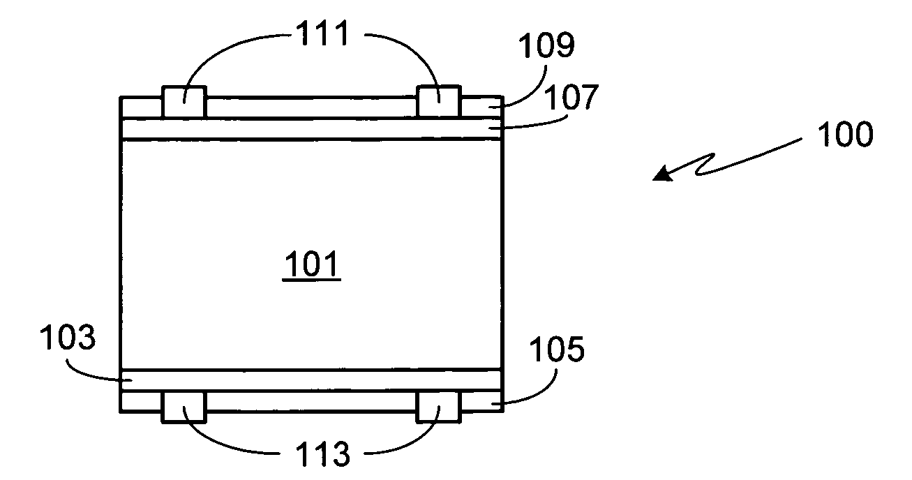
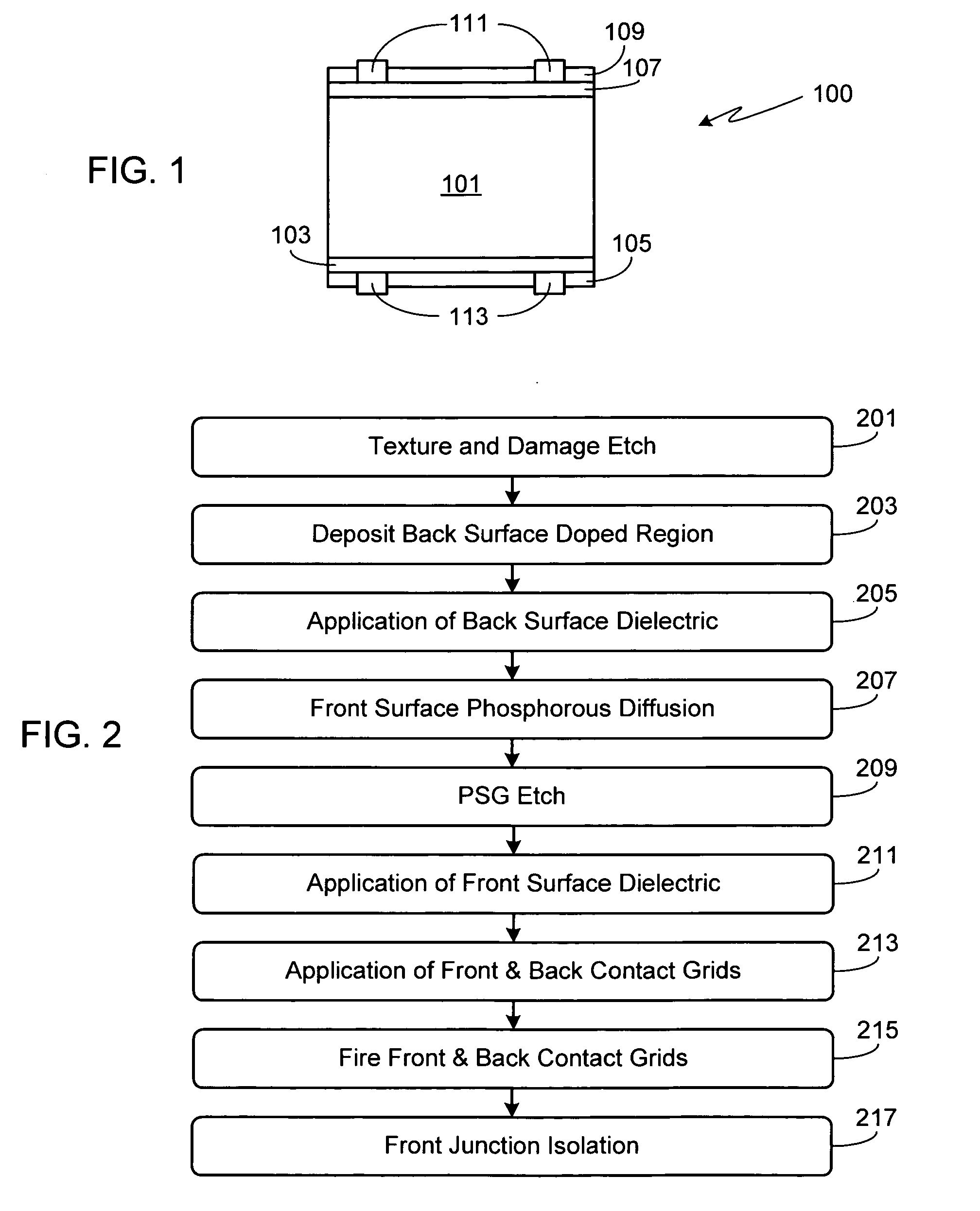
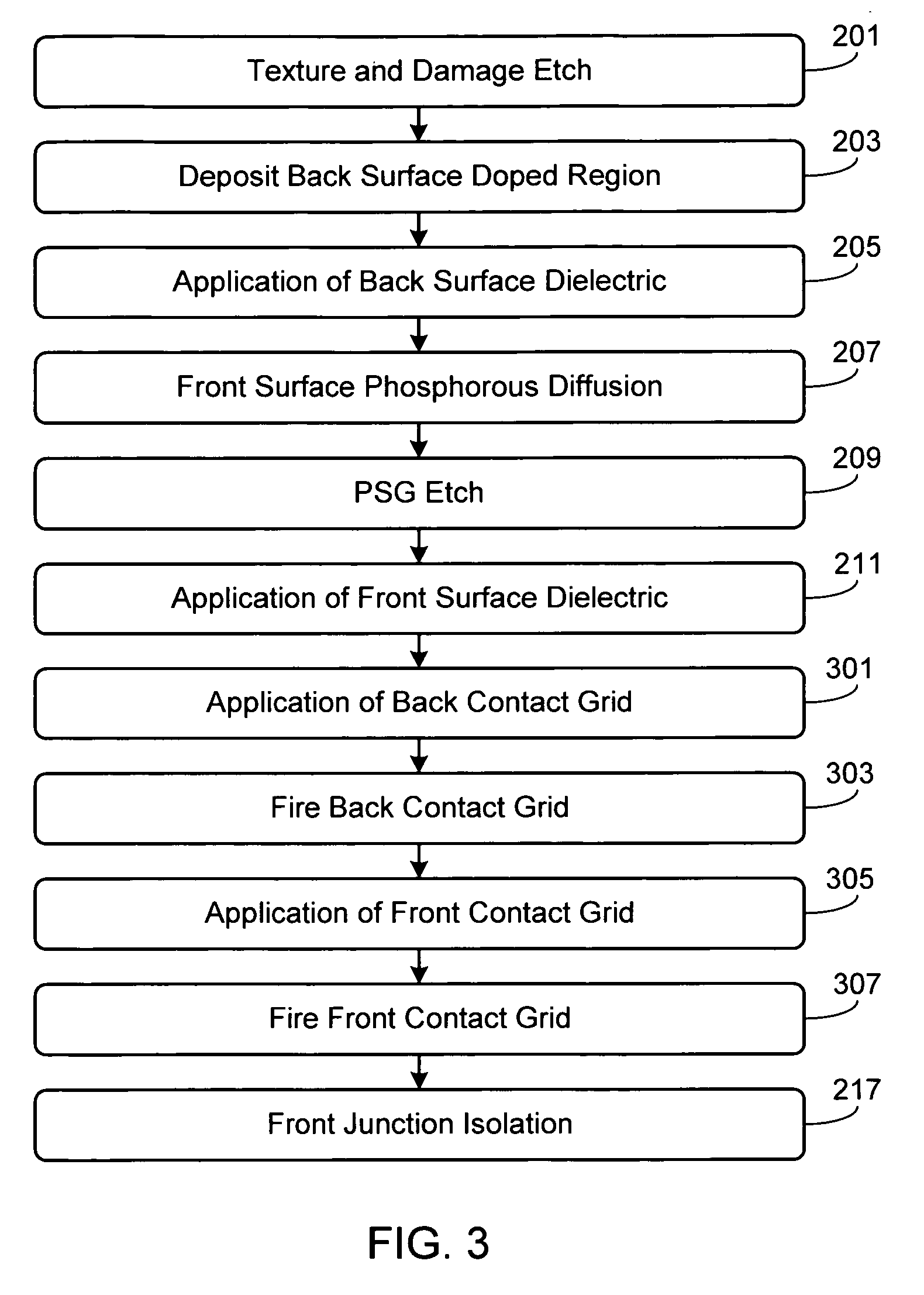
[0013]FIG. 1 illustrates a cross-sectional view of a preferred bifacial solar cell (BSC) structure fabricated in accordance with the procedure described in FIGS. 2 and 3. Silicon substrate 101 may be of either p- or n-type. In the exemplary device and process illustrated in FIGS. 1-3, a p-type substrate is used. Initially, substrate 101 is prepared using any of a variety of well-known substrate preparatory processes (step 201). In general, during step 201 saw and handling induced damage is removed via an etching process, for example using a nitric and hydrofluoric (HF) acid mixture. After substrate preparation, the bottom surface of substrate 101 is doped, thereby forming a back surface doped region 103 (step 203). Region 103 is doped with the same doping type as substrate 101. Increasing the doping level of region 103, compared to substrate 101, lowers the contact resistance. Additionally, doped region 103 reduces back surface recombination and the effects of a positive potential i...


PUM


Abstract

A simplified manufacturing process and the resultant bifacial solar cell (BSC) are provided, the simplified manufacturing process reducing manufacturing costs. The BSC includes an active region located on the front surface of the substrate, formed for example by a phosphorous diffusion step. The back surface includes a doped region, the doped region having the same conductivity as the substrate but with a higher doping level. Contact grids are formed, for example by screen printing. Front junction isolation is accomplished using a laser scribe.

Description

CROSS-REFERENCE TO RELATED APPLICATION[0001]This application claims the benefit of the filing date of U.S. Provisional Patent Application Ser. No. 61 / 215,199, filed May 1, 2009, the disclosure of which is incorporated herein by reference for any and all purposes.FIELD OF THE INVENTION[0002]The present invention relates generally to solar cells and, in particular, to an improved structure and manufacturing process for a bifacial solar cell.BACKGROUND OF THE INVENTION[0003]Bifacial solar cells (BSC) may use any of a variety of different designs to achieve higher efficiencies than those typically obtained by a conventional, monofacial solar cell. One such design is shown in U.S. Pat. No. 5,665,175 which discloses a BSC configuration with first and second active regions formed on the front and back surfaces of the BSC, respectively, the two regions separated by a distance λ. The distance λ allows a leakage current to flow between the first and second active regions, thus allowing a sola...

Claims


Application Information

Patent Timeline
Patent Type & Authority Applications(United States)
IPC IPC(8): H01L31/02H01L31/18
CPCH01L31/022425H01L31/068H01L31/18H01L31/0684Y02E10/547H01L31/1804Y02P70/50
Inventor KAES, MARTINBORDEN, PETEROUNADJELA, KAMELKRAENZL, ANDREASBLOSSE, ALAINKIRSCHT, FRITZ G.
Owner HIGHLAND MATERIALS INC
Why Eureka
Try Eureka