

Method for fabricating a high coercivity hard bias structure for magnetoresistive sensor
- Summary
- Abstract
- Description
- Claims
- Application Information
AI Technical Summary
Benefits of technology
Problems solved by technology
Method used
Image

Examples
first embodiment
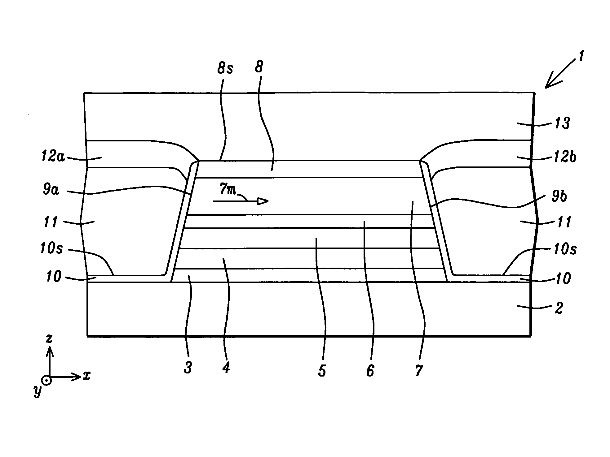
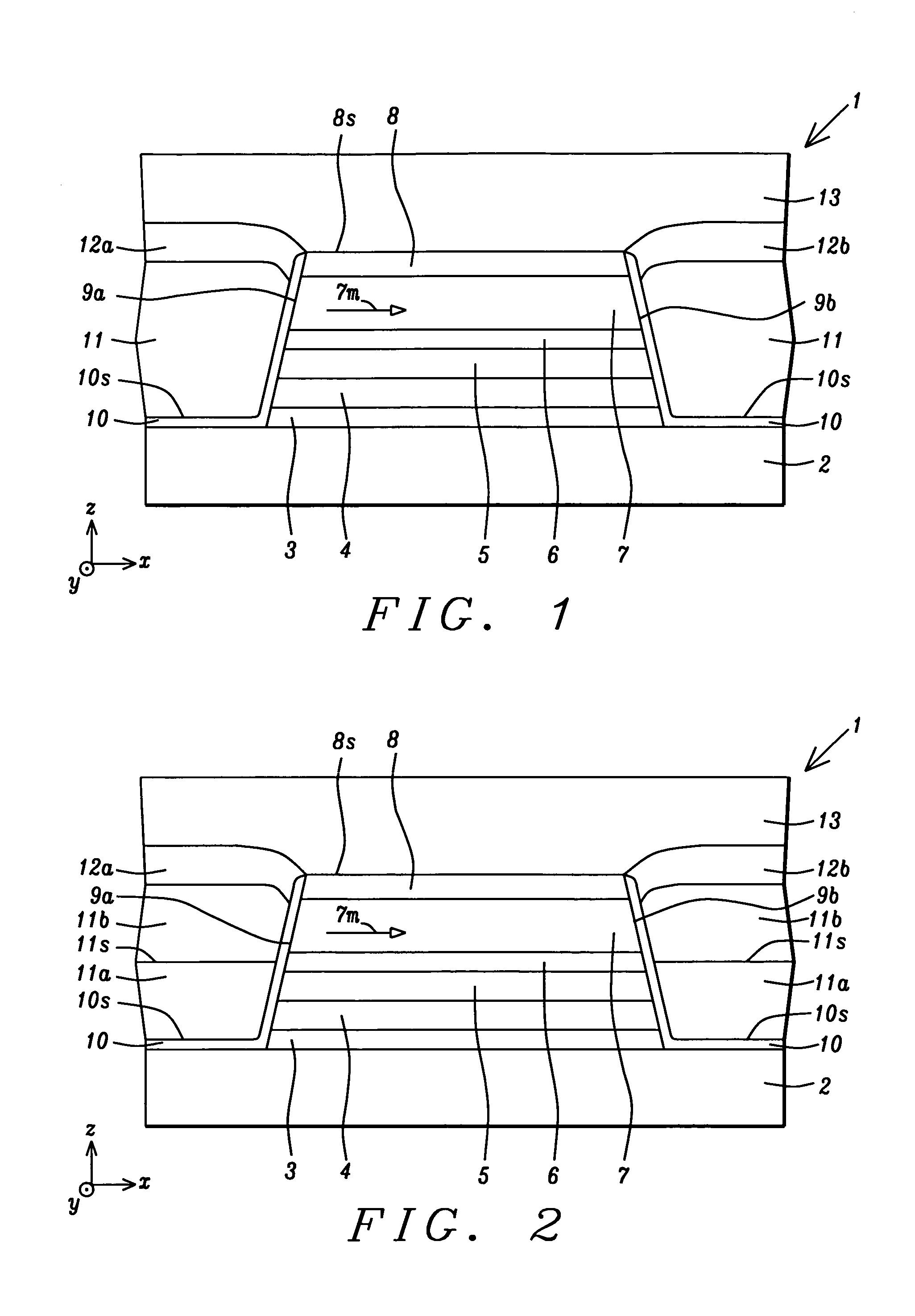
[0018]An important feature according to the present invention is a hard bias structure comprised of seed layer 10 and hard bias layer 11 formed on opposite sides of the sensor structure. The hard bias structure described herein is designed to have a high coercivity in order to stabilize the magnetization of the free layer 7 along an easy axis which is depicted as the (+) or (−) x-axis direction. Preferably, the coercivity of the hard bias layer 11 is substantially greater than 2000 Oe, and more preferably, greater than or equal to about 2300 Oe in order to stabilize a free layer 7 in a sensor, especially in designs where a small sensor is required to meet requirements for a high areal recording density. For example, the hard bias structure prevents stray magnetic fields generated by a magnetic medium from inadvertently switching the magnetization direction of the free layer.
[0019]The seed layer 10 has a thickness between 10 and 100 Angstroms, and preferably about 40 Angstroms, and m...
second embodiment
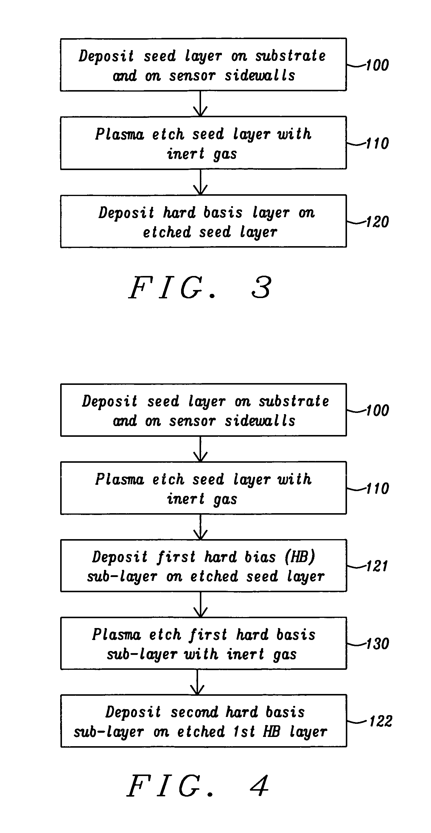
[0028]A process flow diagram for the second embodiment is illustrated in FIG. 4. Steps 100 and 110 are followed as in FIG. 2. Thereafter, in step 121, the first hard bias sub-layer is deposited by an IBD or sputter deposition process. In step 130, the first hard bias sub-layer is mildly etched by a process that may comprise the same conditions as described previously for the seed layer etch. In one aspect, a top portion about 10 to 15 Angstroms thick of the first hard bias sub-layer is removed during step 130 to provide a surface having an increased number of nucleation sites. During step 122, the second hard bias sub-layer is deposited on the etched first hard bias sub-layer. The increased number of nucleation sites on the surface of the etched first sub-layer is responsible for promoting a smaller average grain size in the second hard bias sub-layer formed in step 122, especially in a lower portion of the second sub-layer formed along the interface with the first hard bias sub-lay...
PUM
| Property | Measurement | Unit |
|---|---|---|
| Temperature | aaaaa | aaaaa |
| Temperature | aaaaa | aaaaa |
| Time | aaaaa | aaaaa |
Abstract
Description
Claims
Application Information